How to Manufacture a Solar Cell: Process, Machines, and Difficulty
Table of Contents
Quick answer: a solar cell is manufactured from a purchased wafer through seven process blocks – incoming wafer inspection, texturing, doping and junction formation, edge isolation, anti-reflective coating, metallisation, and sorting and binning. Each block is a separate machine class, and most of them run wet chemistry or a high-temperature step that a module line does not contain at all. Making a solar cell yourself at home is a completely different activity: it means buying finished cells and soldering them into a small panel, or building a dye-sensitised or perovskite demonstrator that has no relationship to factory cell production. Anyone budgeting a factory needs to hold one distinction firmly: cell manufacturing and module assembly are two separate industries with different capital, different chemistry and different failure modes.
Why Cell Manufacturing Is a Different Business from Module Assembly
A module line buys cells and puts them together. Its material list is cells, ribbon, flux, glass, encapsulant, backsheet or rear glass, frame and junction box, and its process is mechanical and thermal: solder, place, laminate, frame, test. A cell line buys wafers and turns them into something electrically active. Its material list is wafers, process chemicals, dopant sources, process gases, cleaning agents and metallisation pastes, and its process is wet chemistry, high-temperature diffusion and thin-film deposition.
The two businesses also fail in different ways. In module assembly the dominant loss is breakage and rework, and material dominates the cost structure – the machines are a modest slice of the total. In cell manufacturing, material is still large but the line itself is much more expensive, and the real exposure is yield and efficiency distribution. A cell line does not merely have to produce cells. It has to produce cells inside a narrow bin, because a cell that is 0.3% below the target bin loses value permanently the moment it is printed on the sorter.
That is the difference most first-time entrants underestimate. A module factory that runs badly makes fewer modules. A cell factory that runs badly makes cells nobody wants to buy, and the loss is already locked into the wafer before anyone notices. Our separate article on solar cell versus solar panel manufacturing covers the commercial side of that split in more detail.
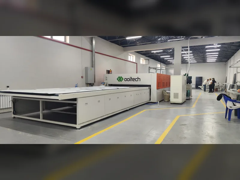
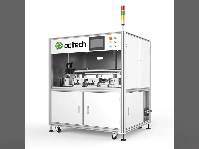
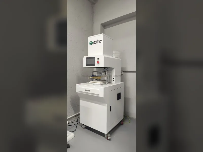
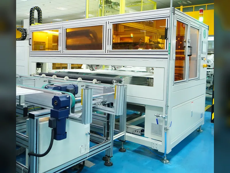
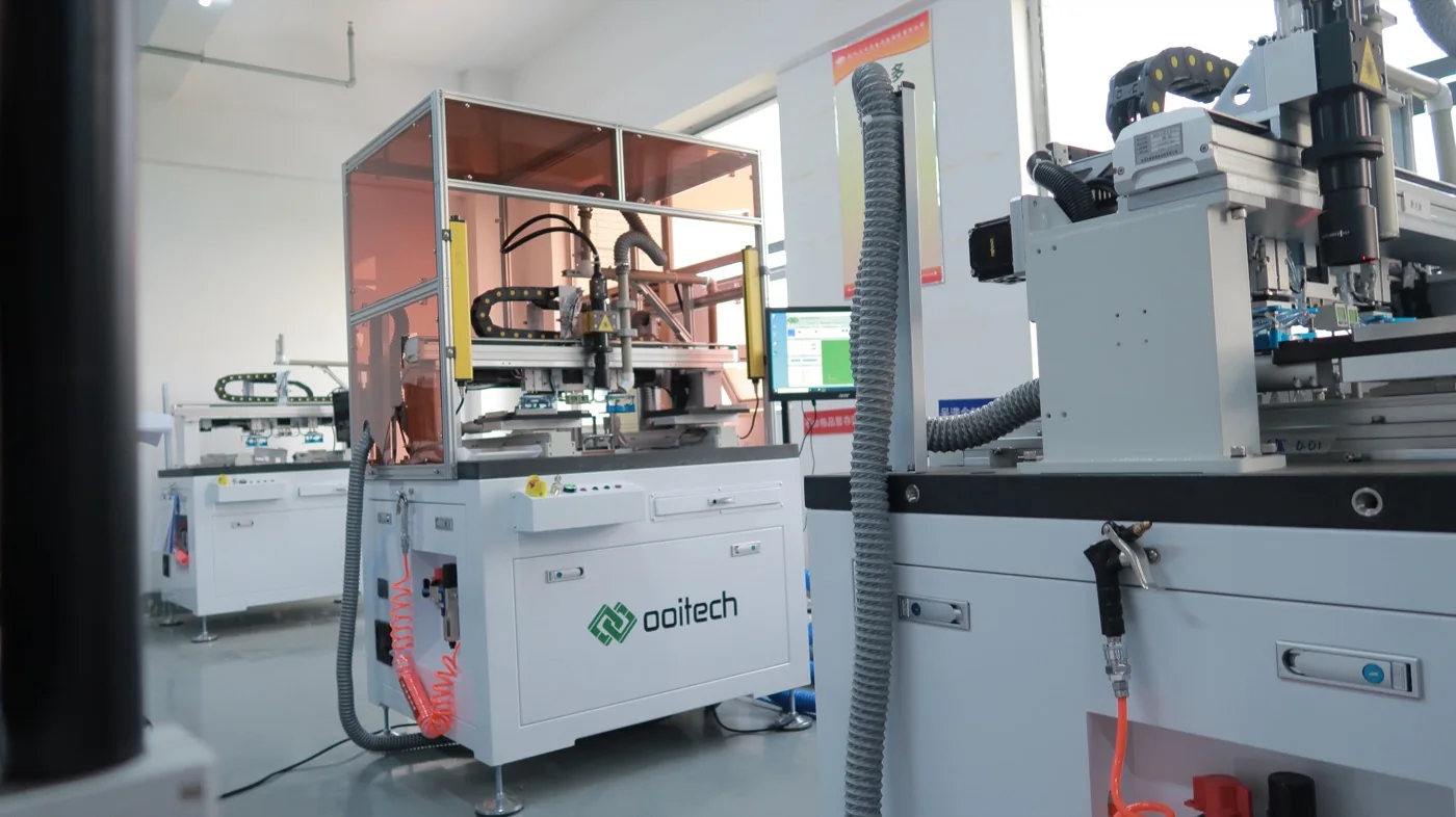
Cell processing looks like this from the outside: an automated workstation with controlled handling, not a bench where a module is assembled.
The Cell Process from Wafer to Sorted Cell
The table below is the whole route at a glance. Every row is a station, and every station has one parameter that decides whether the output is sellable. The sections after it explain what each one is actually doing.
| Process block | What it does | Equipment category | Key control parameter |
|---|---|---|---|
| Incoming wafer | Confirms resistivity, thickness, dimensions and saw-damage state before any value is added | Wafer inspection and sorting station | Resistivity range, thickness tolerance, total thickness variation |
| Texturing and cleaning | Etches random pyramids into the surface to trap light and removes saw damage | Wet bench – texture and clean | Bath temperature and concentration, etch depth, resulting reflectance |
| Doping and junction formation | Creates the p-n junction, or the passivating contact stack on an n-type route | Diffusion furnace, LPCVD or PECVD for the TOPCon stack, ion implanter | Sheet resistance, junction depth, temperature uniformity across the boat |
| Edge isolation | Removes the conductive path that diffusion leaves around the wafer edge, which would otherwise shunt the cell | Laser edge isolation, or wet or plasma etch | Isolation depth and width, resulting shunt resistance |
| Anti-reflective coating | Cuts front-surface reflection and adds surface passivation | PECVD for silicon nitride, ALD for aluminium oxide on the rear | Layer thickness, refractive index, uniformity across the carrier |
| Metallisation | Prints and fires the current-collecting grid on the front and the pads on the rear | Screen printer plus drying and firing furnace, or plating for some routes | Paste deposit weight, print alignment, firing peak temperature and belt profile |
| Sorting and binning | Measures each finished cell and separates it into efficiency and current bins | Cell tester and sorter, with electroluminescence inspection | Calibration of the reference cell, bin boundary definitions |
Step by Step: What Each Station Does and What It Controls
Incoming wafer: the specification decides everything downstream
Cell manufacturing starts with a wafer you buy, not a wafer you make. That single fact is the reason a cell line is more accessible than a wafer line and far less accessible than a module line. The incoming wafer decides the achievable efficiency ceiling: resistivity sets the doping design, thickness sets the mechanical budget the handling system has to respect, and surface condition decides how the texture step behaves. A wafer incoming inspection station is not a quality luxury; it is the only place where a bad lot can be rejected before you have spent money processing it.
Texturing: the step that looks trivial and is not
In an alkaline texture bath, the wafer grows a random pyramid surface that bounces incoming light back onto itself instead of straight out of the cell. The equipment is a wet bench with heated baths and a rinse and dry section, and the process window is narrow: bath temperature, chemical concentration and residence time all move the pyramid size, and pyramid size moves reflectance. Texturing is also where a line first shows whether its chemical dosing control is real or nominal. The same optical idea appears on the module side in why solar panel glass is textured, though the mechanism there is a rolled pattern rather than a chemical etch.
Doping and diffusion, and the TOPCon fork
For a classic p-type route, wafers go into a diffusion furnace where phosphorus diffuses into the surface and forms the emitter. The control parameter is sheet resistance, measured after the step, and it has to be uniform not only across one wafer but across the whole boat and from batch to batch. For an n-type TOPCon route the process changes shape: the rear side needs an ultrathin tunnel oxide plus a doped polysilicon layer, deposited by LPCVD or PECVD, and that stack is what makes the cell sensitive to the metallisation step later. The structural differences between the two rear-side designs are set out in TOPCon versus BC cell backside comparison.
Edge isolation and rear-side clean-up
Diffusion does not respect the edge of the wafer. Phosphorus wraps around the perimeter and creates a conductive bridge from the front emitter to the base, which shunts the finished cell. Edge isolation removes that bridge, either with a laser scribe around the perimeter or with a wet or plasma etch that strips the edge and the rear parasitic layer. The parameter to watch is the resulting shunt resistance on the finished cell; a drifting laser focus or a contaminated etch bath shows up here first, and it shows up as a whole batch of low-efficiency cells rather than an obvious defect.
Anti-reflective coating and surface passivation
The texture reduces reflection but does not eliminate it. A silicon nitride layer deposited by PECVD brings front reflectance down further and simultaneously passivates the surface, reducing recombination. On high-efficiency n-type routes an aluminium oxide layer deposited by ALD handles rear passivation, often with a nitride cap. The controls are film thickness and refractive index, both of which have to be uniform across the carrier, and both of which are measured optically. This is the first genuinely thin-film step in the flow, and it is where a line with weak process control starts producing cells that look fine and test low.
Metallisation: screen printing, drying and firing
Metallisation is the most expensive process block after the wafer itself, because the front grid is made from silver paste. A screen printer deposits the paste pattern, a drying step removes solvent, and a firing furnace takes the wafer through a controlled thermal profile that burns through the anti-reflective coating and forms an ohmic contact with the silicon. Three parameters dominate: deposit weight, which is money, print alignment, which decides whether the fingers land on the intended lines at increasing busbar counts, and the firing profile, which decides contact quality and whether the paste damages the junction underneath. The chemistry between paste and silicon is subtle enough to have its own article – see how silver paste bites through polysilicon on the TOPCon rear side.
Sorting, binning and testing
The last block measures every cell under a calibrated simulator, records current and voltage at the maximum power point, checks appearance, and frequently runs electroluminescence imaging to catch cracks and inactive areas. Cells are then sorted into bins. This is not a formality. The cell tester is the price-setting instrument for the whole factory, because a bin is a promise to the customer, and a tester that drifts silently reprices your entire output. Module lines run their own inspections for the same reason, as covered in EL testing for solar panels: inline versus offline setup.
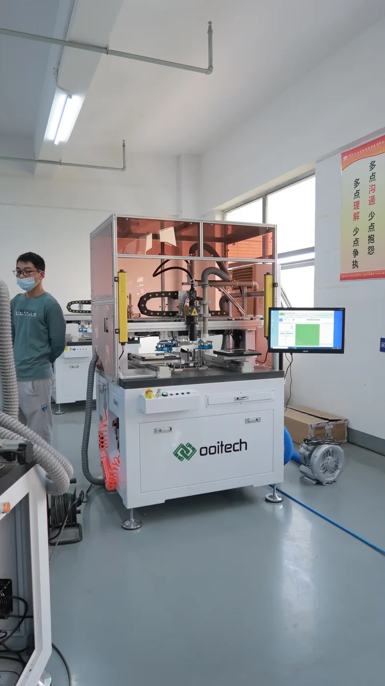
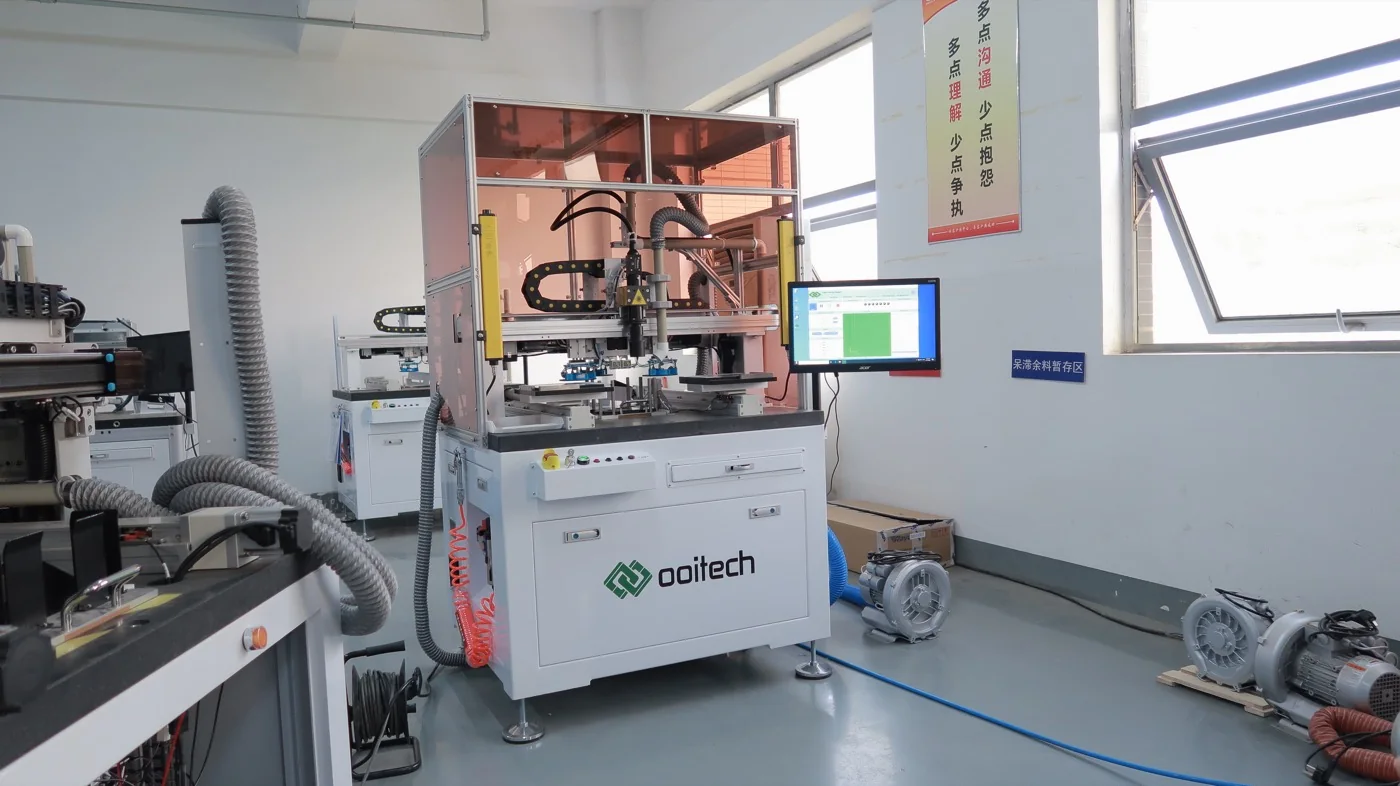
Enclosed handling stations of this kind are the reason cell yield depends on process control rather than on buying a longer machine list.
Where the Difficulty Actually Sits
Three things make cell manufacturing hard, and none of them is the machine catalogue.
The first is chemistry. Texturing, cleaning, diffusion, edge isolation and coating are all processes where the result depends on a bath or a gas environment that drifts continuously. Keeping them in control means continuous measurement, chemical analysis, dosing discipline and a maintenance culture. A module line can be run by operators who follow a mechanical procedure. A cell line cannot.
The second is yield sensitivity. Because value accumulates across the route, a defect introduced at texturing is only discovered at the tester, several hours and several process steps later. Feedback loops are long, and by the time a problem is visible, a large volume of material has already been through the line. Handling breakage compounds it: thinner wafers and more automation mean the mechanical budget shrinks while throughput rises.
The third is that the efficiency distribution is the product. Two lines with identical machines can produce different revenue per wafer, because one holds a tighter distribution and the other spreads across three bins. Tightening that distribution is a process-control problem, not a purchasing problem, and it takes months of tuning after commissioning.
The Capital and Yield Barrier in Plain Terms
A cell line is a different order of investment from a module line at the same nominal capacity. It needs wet benches with chemical delivery and waste treatment, furnaces with gas handling and exhaust systems, vacuum deposition tools, a printing line with paste management, a calibrated tester, and a building with the utilities and environmental permits all of that implies. Chemical storage, effluent neutralisation and safety systems are not optional line items; they are conditions of operating legally in most jurisdictions.
The comparison that matters for a business plan is cost per unit of capacity and time to stable yield. On both measures a cell line is substantially heavier, and it does not scale down gracefully – there is a practical floor below which the wet chemistry and gas infrastructure cannot be justified. For the wider cost picture on the module side, including how different capacity tiers are quoted, see solar panel production line cost by capacity. That article is deliberately about module lines: it is the entry point this article is arguing you should take.
Why a First-Time Entrant Should Start with Module Assembly
A module line is a legitimate manufacturing business, not a consolation prize. It buys a globally traded input, adds mechanical and thermal value, and sells a branded product with a warranty. Its process is largely reversible in the sense that problems are visible at the station where they occur, and its equipment is standardised enough that a new team can reach stable output in a reasonable ramp.
More importantly, it puts you inside the supply chain. A module maker buys cells every month, learns which bins and formats actually perform, and builds the commercial relationships that a cell venture would need anyway. If the plan is eventually to move upstream, the module line is the cheapest possible education in what the customer downstream of a cell factory actually cares about. The step-by-step version of that entry path is in how to start a solar panel manufacturing business, and the machine-level process map is in the ten-step module manufacturing process. This article deliberately does not repeat either.
What It Takes to Make a Solar Cell Yourself
The people searching for how to make their own solar cell are usually not planning a factory. They want to build something at home, and the honest answer has two branches.
The practical branch is to buy finished cells – typically sorted, tabbed or untabbed, sold in small lots – and assemble them into a small panel with ribbon, flux, encapsulant and a frame, then test it. That is module assembly at hobby scale, and it teaches the real lesson: the cell is the hard part, and it arrives finished. A workshop that goes through this exercise usually comes away with a much sharper appreciation of why cell production is a separate industry.
The experimental branch is a laboratory demonstrator: dye-sensitised cells built from titanium dioxide, a natural dye and an electrolyte, or a perovskite cell made in a glovebox with spin coating. These are genuine photovoltaic devices and genuinely interesting to build, and none of them is a route to a production line. The materials, the deposition methods, the encapsulation and the stability requirements are all different from silicon manufacturing. Build one to understand the physics; do not build one to plan a business.
What Ooitech Supplies and What It Does Not
Ooitech builds module production lines from 5 MW to 600 MW, semi-automatic through fully automatic, covering stringing, layup and bussing, lamination, framing, glue dispensing and end-of-line testing, along with cell handling and singulation equipment used around cell processing. The company does not offer a turnkey diffusion and wet-chemistry cell line, and this article is not a suggestion that it does. If your plan is a cell factory, the realistic route is a technology partnership with an established cell producer plus a specialist integrator for the wet and furnace sections – and a very different capital plan from the one a module line needs.
Frequently Asked Questions
How is a solar cell manufactured, in one sentence?
A purchased silicon wafer is textured and cleaned, doped to form a junction, edge-isolated, coated with an anti-reflective and passivating layer, printed with a silver grid and fired, then tested and sorted into an efficiency bin. Each of those steps is a separate machine class with its own control parameter.
Can I make a solar cell at home?
You can assemble a small panel from bought cells, and you can build a dye-sensitised or perovskite demonstrator in a workshop or laboratory. What you cannot do at home is replicate the industrial route, because texturing, diffusion and firing all need controlled chemistry and high-temperature equipment with gas handling and waste treatment.
Why is cell manufacturing harder than module assembly?
The process is chemistry-based rather than mechanical, so it drifts continuously and needs active control. Defects are discovered hours after they are created, so feedback is slow, and the product is an efficiency distribution rather than a count of finished units. The equipment is also far more expensive at the same nominal capacity.
What is the most expensive step in making a cell?
The wafer you buy is the largest single input, followed by the silver paste used in metallisation. Everything else – chemicals, gases, energy, labour and depreciation – matters, but those two dominate the cost of a finished cell before yield is taken into account.
Which machines does a cell line need that a module line does not?
Wet benches for texture and clean, a diffusion furnace or a deposition tool for the passivating contact stack, an edge isolation system, PECVD and often ALD for coating, a screen printing line with a firing furnace, and a calibrated cell tester and sorter. A module line needs none of these; it starts at the stringer.
Does TOPCon change the cell manufacturing process much?
Yes. The n-type TOPCon route replaces the simple rear-side design with an ultrathin tunnel oxide and a doped polysilicon layer, which adds deposition equipment and makes the rear metallisation step considerably more delicate. The front-end blocks – texture, clean, edge isolation – remain broadly similar.
Should a first factory be a cell line or a module line?
Almost always a module line. It has a lower capital floor, a shorter ramp to stable output, and it puts you in the market buying cells monthly, which is the best available education if you later want to move upstream. Start a cell line only with an experienced technology partner and a capital plan that survives a long yield ramp.