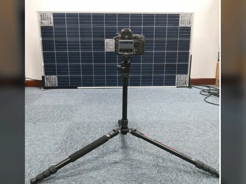
Quick answer: The Portable HD EL Tester is built for laboratories and production environments where solar module types vary in size and format. It captures electroluminescence images at resolutions down to about 0.2 mm defect detection, and is designed to be moved to the module rather than requiring the module to be brought to a fixed chamber. That portability matters in three situations: incoming inspection of modules on a rack, field inspection of installed arrays, and laboratory work where modules arrive in ones and twos rather than as a production flow. Electroluminescence shows micro-cracks, finger interruptions and soldering defects that a power measurement cannot detect, which is why a portable unit is useful wherever a fixed inline chamber is not justified.
PV Module Manufacturing · by Jerry, Ooitech
Product Introduction

The Portable HD EL Tester is built for laboratories and production environments where solar module types vary in size and version changes happen frequently. Traditional single-camera testers and multi-camera stitching systems can be hard to adapt in such conditions, so this unit uses a single camera with auto focus to deliver sharp, clear images without manual adjustment.
The device produces high resolution electroluminescence images that reveal micro cracks, broken fingers, black cores, mismatched cells and other hidden defects inside solar cells and modules. Spatial resolution can be verified directly through a test chart, making the tester suitable for R&D labs, quality inspection teams, and on-site service engineers handling different cell technologies such as PERC, TOPCon, HJT, IBC, MBB and shingled modules.
It is compact, lightweight, and easy to move between workstations. No fixed dark room is required, and the operator can connect to a laptop, tablet or smartphone within minutes.
Technical Specifications

| Item | Parameter |
|---|
| Model | YH-EL |
| Effective Pixels | 24 Megapixel |
| Lens | Infrared lens, auto focus |
| Focal Length | 18-55mm |
| Exposure Time | 1-60s adjustable |
| Vignetting Correction | Yes |
| Data Transmission | USB3.0 / WiFi |
| Distortion Correction | Yes |
| Sensor Size | 23.5 x 15.6 mm |
| ISO Sensitivity | 100-25600 |
| Minimum Crack Width Detection | 0.2mm |
Technical Advantages
Auto focus infrared lens: no manual focusing required, saves time when switching between different module sizes
24MP high resolution: captures fine defects down to 0.2mm crack width
Wide exposure range: 1-60s adjustable exposure suits different cell technologies and module layers
Flexible connectivity: USB3.0 cable for stable wired transfer or WiFi for wireless use with PC, tablet or mobile phone
Built-in correction: vignetting and distortion correction ensure uniform brightness and accurate geometry across the whole image
Compact design: portable body, no dedicated space needed, easy to carry to customer sites or between lines
Practical software tools: exposure time and gain setting, contrast stretching, and image cropping for clearer defect analysis
Product Application

The portable EL tester is widely used in scenarios where speed, flexibility and image clarity all matter:
Solar module R&D laboratories testing many different cell types and module sizes
Quality control on solar panel production lines for incoming, mid-process and outgoing inspection
Field inspection of installed PV plants to check transportation damage, hot spots and hidden cracks
Third party testing services and certification support
After-sales and warranty claim verification for solar modules
Training centers demonstrating EL imaging principles and defect identification
It works with mainstream module formats including G1, M6, M10, M12 cells, PERC, TOPCon, IBC, HPBC, MBB and shingled modules, as well as flexible, thin film, CIGS and CdTe panels.
How to Use and Order
Operation is straightforward:
Place the module in a dark environment and connect the EL power supply
Connect the tester to a PC via USB3.0, or pair with a laptop, tablet or phone over WiFi
Open the software, set exposure time and gain, then capture the EL image
Use contrast stretching and cropping tools to review cracks and defects
For quotation, technical drawings, software demo or customization based on your module size and workflow, please send your module specification and testing requirements so a matching configuration can be prepared.
Related: Why bussing (overlap soldering) causes cell cracks is what that crack looks like after lamination, and why it is read in EL rather than by eye.
Related: Hot spots, microcracks and PID: three slow module failures is the other instrument an inspection pairs it with.
Related: How a solar panel is made: every step and every check is the instrument used for that check away from the line.