Why Bussing (Overlap Soldering) Causes Cell Cracks
Table of Contents
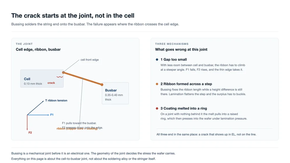
Quick answer: A centre-hole crack that comes out of the bussing step is a mechanical failure at the joint between the cell edge and the busbar. Three things cause it. The reserved gap between cell and busbar is too small, so the ribbon crosses at a steep angle and presses down on the edge. The ribbon was formed across a height difference that lamination later flattens, leaving surplus ribbon that has to buckle somewhere. Or the ribbon coating melted into a raised solder ring that is pressed into the wafer. All three load the edge of a wafer roughly 0.13 mm thick, and all three usually show up only after lamination, in electroluminescence.
Centre-hole cracks are among the most frequent cosmetic defects a module line produces, and the list of possible causes is long. Handling damage, glass, encapsulant, stringer faults and lamination parameters all have their own signatures. This page narrows the topic to the part of it that comes from bussing — the overlap soldering step that joins a string end onto a busbar — and walks through the three ways that step breaks cells.
What these three have in common is that none of them is an electrical failure. They are geometry problems. The joint between a cell edge and a busbar is a place where a thin wafer, a much thicker strip of ribbon and a solder joint meet, and where a strip under tension changes direction. Get that geometry wrong by a few tenths of a millimetre and the wafer pays for it later, in the press.
Below is the mechanism for each of the three causes, what distinguishes them from one another on the line, and what is worth measuring before lamination rather than after.
The joint this page is about
Bussing is where the ends of a finished string are soldered onto the busbar that collects the current and carries it out to the junction box. On a TOPCon string the ribbon leaves the front of the cell and is soldered to the back of the busbar, so the joint sits at the cell edge rather than in the middle of a cell surface.
The fixture brings the cell and the busbar to a common plane during the operation. That does not make them the same thickness, and the difference is not small:
| Item | Typical thickness |
|---|---|
| TOPCon wafer | 0.13 mm |
| Centre busbar ribbon | 0.35 mm to 0.40 mm |
So the ribbon leaves a 0.13 mm wafer, crosses a gap, and lands on a strip roughly three times as thick. The ribbon is the only member that spans that step, and it does so under tension. Where it touches the cell edge, it pushes. That is the whole failure mode in one sentence; the three causes below are just three ways of making the push bigger.
Cause one: the reserved gap between cell edge and busbar is too small
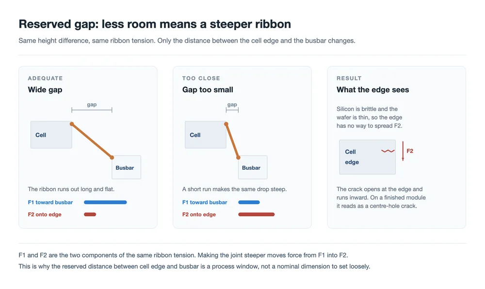
The gap between the cell edge and the busbar is a process window, not a nominal dimension. Several ordinary things push the cell edge closer to the busbar than it should be. A CCD vision offset on the bussing machine can do it. So can a positioning fault on the same machine. A string whose total length has drifted out of tolerance does it too, because the end cell then arrives somewhere other than where the fixture expects it.
Once the gap is short, the ribbon has to make the same climb over a shorter run, so the angle between the ribbon and the wafer edge gets steeper. Take the ribbon tension as roughly constant and split it into two components at the point where the ribbon leaves the cell:
- F1 acts in the plane of the wafer, pulling the ribbon toward the busbar.
- F2 acts perpendicular to the wafer, pressing the ribbon down onto the cell edge.
A steeper crossing moves tension out of F1 and into F2. The horizontal pull falls, the downward pressure rises, and the edge is where that pressure arrives. Silicon is brittle, the wafer is thin, and the edge is a free surface with no material around it to spread the load. A crack starts at the edge and runs inward. On a finished module it reads as a dark line or a dark patch in EL.
This cause is the easiest of the three to prevent and the hardest to see, because a joint that is 0.2 mm out of position looks perfectly normal. The control is the placement itself: vision calibration, the positioning repeatability of the bussing head, and the length tolerance of the string arriving from the stringer.
Cause two: the ribbon was formed across a step that lamination removes
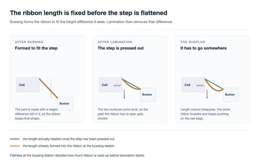
The second cause starts the same way, with a height difference between cell and busbar at the bussing station, but the outcome is different. Here the difference is large enough that the ribbon, once soldered, keeps a step in its shape. The joint is made, the ribbon is fixed, and the length of ribbon in that joint is now a fixed quantity.
Lamination then does what lamination does: it presses the assembly flat. The two surfaces come level, and the path the ribbon has to span between them gets shorter. The ribbon, however, is already the length it is, and it cannot shorten. The surplus has to go somewhere, so the ribbon buckles — and the buckle is sitting on the cell edge.
The result is the same defect as cause one, with a different signature: it tends to appear in batches rather than as isolated cells, because the step is a property of the setup rather than of one joint. It is also the reason a joint can pass inspection at the bussing station and still seed cracks in the press. Coplanarity at bussing is the control point, not the appearance of the joint.
Cause three: the coating melted into a raised ring
The third cause is the rarest, it is the most instructive, and it is the only one that starts as a purchasing decision. It appeared in the source case as a line with persistent post-lamination centre-hole cracks. Several laminators were producing the same defect and the bussing machine was the one fixed element in the picture, which is what pointed the investigation at the bussing step.
What was happening there: the cell and the busbar had a slight height difference, and in the fork area, where the busbar splits toward the leads, there was no busbar under the ribbon to weld against. The ribbon separated from the wafer. The soldering heat then melted the ribbon coating, which drew itself into a bead around the ribbon and froze as a raised ring. Under lamination pressure that ring acted as a hard point on top of a brittle wafer, and cracked it.
The reason the rings appeared in batches is the part worth remembering. The line had switched to a lower-cost ribbon with a high tin and low copper content, and the coating on that ribbon varied in thickness along the coil. More solder at the joint produced a bigger ring. Returning to standard ribbon cleared the defect completely.

Two points follow from that. Coating thickness and its uniformity belong in incoming inspection rather than on a datasheet alone. the coating is the part of the ribbon that does the joining, and a coil with uneven coating behaves differently from an even one, even when both meet the same average figure. And a joint needs something behind it. Where the ribbon crosses an area with no support underneath, both the soldering and the lamination are working against geometry rather than with it.
Telling the three apart
On a line producing centre-hole cracks, the pattern of the defect is often enough to point at the cause before any measurement is taken. The three below are the bussing-related signatures; other signatures exist and point elsewhere.
| What you see | Likely cause | First thing to check |
|---|---|---|
| Cracks that follow the busbar run, appearing across cells whose joints all look acceptable | Reserved gap too small | Vision calibration and the actual gap at the joint |
| Batch cracks that track a setup change rather than a shift | Ribbon formed across a step | Coplanarity of cell and busbar at bussing |
| The same defect on several laminators while one bussing machine stays constant | Solder ring | Support under the ribbon, then the ribbon coating spec |
The third row is the one worth internalising. When a defect follows the part of the line that did not change, the part that did not change may be the cause, not the control.
What to hold at the bussing station
None of the three causes can be inspected away after lamination. They have to be held at the station that makes the joint, and on a bussing machine that means four things:
- Placement. The gap between cell edge and busbar should be measured and charted, not assumed from the program. Vision offsets and string length drift both move it.
- Coplanarity. The height difference between cell and busbar at the moment of soldering is what fixes the ribbon length. Support tooling and fixture flatness decide it.
- Ribbon specification. Coating thickness and its uniformity, checked on incoming material rather than read off the datasheet. The structure of the ribbon and its coating determine how much solder ends up in the joint.
- Inspection timing. Electroluminescence after lamination is where these defects appear. If your EL check runs earlier in the flow, the crack will be missed at the point where it is still traceable to a station.
The lamination side matters too, but mostly as an amplifier. A press that flattens the assembly evenly, with the vacuum stages and pressure ramp doing what they are supposed to, treats every joint the same way. The lamination cycle is where the geometry built at bussing finally meets its consequences.
Frequently asked questions
Why does the crack only appear after lamination?
Because the load that breaks the edge is applied in the press. The joint itself looks normal when it is made; the surplus ribbon has not buckled yet, and the solder ring is not under pressure yet. Damage that is already in the wafer can also stay closed until the pressure of lamination opens it into a readable crack in EL.
Why is it called a centre-hole crack?
The name comes from where the defect is seen on the finished module. The mechanical origin is the cell-to-busbar joint, which is why the three causes on this page all point back to the bussing step rather than to the hole itself.
Is this a ribbon problem or a soldering problem?
It is a geometry problem that shows up through a soldered joint. Causes one and two have almost nothing to do with the ribbon as a product: the gap and the height difference are properties of how the parts are placed and supported. Cause three is the exception, and there the ribbon's coating is directly involved.
Would a thicker ribbon help?
It would raise the step the ribbon has to cross at the busbar, and it would put more material into any ring that forms. The direction that helps the edge is the opposite one: a smaller and better controlled step, a gap held inside its window, and a coating that behaves the same way along the whole coil.
Can any of this be caught before lamination?
Two of the three can, and only by measurement. The reserved gap is a dimension you can check at the joint. Coplanarity at bussing is a dimension you can check on the fixture. The solder ring can be seen on the joint if someone looks for it, which is why it is worth having an inspection step after bussing as well as after lamination.
Does this apply to busbarless modules?
The mechanism changes with the joint. On a 0BB module the ribbon is bonded directly to fine fingers, so there is no busbar edge to cross and the joint loads are distributed over far more, much smaller connections. The busbar joint described here is the one where a single thick strip crosses a thin wafer edge.
Final thoughts
Three different stories end in the same dark line in EL, and the reason they are worth separating is that they call for three different fixes. The gap is a placement problem. The step is a flatness problem. The ring is a materials and support problem. A line that treats all three as "lamination trouble" will spend its time adjusting a press that is not the cause.
The common thread is that a strip of ribbon under tension is a load path, and the wafer edge is the narrowest point on it. Thin cells have made that edge narrower, and the operating window that used to absorb a tenth of a millimetre of misalignment no longer does.
Related reading: What a PV ribbon does: three jobs, one trade-off · PV ribbon materials: copper core, hardness and coating · PV ribbon structure and types: flat, round and shaped · DH200-Y automatic bussing machine · HDX200-P half-cell bussing machine · SAW-100A layup and bussing machine · Solar panel laminator: lamination process explained · How to choose the right solar module laminator · PV module reliability tests: cell vs module failure causes · Tabber and stringer machine: how it works, how to choose
Thickness figures for the wafer and the centre busbar are the typical values quoted in the source material and vary by supplier and design. References to the ribbon tension components F1 and F2 describe the direction of the load at the joint; the split between them follows from the angle of the ribbon and is not a measured value.
Related: Hot spots, microcracks and PID: three slow module failures puts that joint defect into the wider picture of gradual module loss.
Related: Solar cell stringer mechanisms: a zone-by-zone guide. The bussing joint fails downstream of the stringer, on the joint the stringer made.
Further reading and background data
Public reference material on this topic, published by the organisations that maintain the industry's technology roadmap and market data: