26.2% Certified Efficiency Breakthrough
Table of Contents
Quick answer: An all-perovskite tandem solar module has reached 26.2% certified efficiency, a result that matters because all-perovskite avoids the silicon bottom cell entirely. The module demonstrated an open-circuit voltage around 2.182 V, which is close to double a single-junction silicon cell and is the signature of two junctions in series. The certification testing included damp-heat exposure at 85 °C and IEC 61215 mechanical requirements, with a 5 mm to 30 mm class test geometry. Perovskite tandem has historically failed on stability rather than efficiency, and that is what makes a certified result different from a laboratory record. The remaining gap to production is area: most records are on small modules, and scaling a perovskite coating to a full-size module without pinholes and uniformity loss is a separate engineering problem.
PV Module Manufacturing · by Jerry, Ooitech
Introduction
All-perovskite tandem solar modules are widely regarded as a strong contender for next-generation photovoltaic technology thanks to their high efficiency and low-cost potential. Yet large-area commercialization has been seriously held back. While small-area devices have already crossed 30% efficiency, large-area modules (≥20 cm²) have long been stuck around 24.5%. The main culprits are the strong near-infrared parasitic absorption and interfacial thermal instability of the Au/PEDOT:PSS structure in conventional gold-based tunnel recombination junctions (TRJs), together with degraded charge transport in large-area Pb-Sn perovskite films caused by non-uniform crystallization during blade coating.
This study develops a solution-processed TRJ built on surface-engineered In₂O₃ nanocrystals. By tuning nanocrystal morphology and surface chemistry, the team achieved high optical transparency, smooth interfaces, and ideal energy-level alignment. At the same time, phosphonic-acid-type additives were introduced into the Pb-Sn perovskite precursor to improve electronic contact with the In₂O₃ recombination layer, enhance hole extraction, and tune crystallization kinetics to relieve residual strain in large-area films. This combined strategy simultaneously boosts carrier recombination efficiency at the junction, charge extraction, and large-area film uniformity, ultimately delivering a JET-certified 26.2% efficiency over a 65 cm² aperture area (VOC = 2.182 V, FF = 77.4%, JSC = 15.6 mA cm⁻²) — a key milestone on the road to scaling up all-perovskite tandem photovoltaics.
Design and Advantages of the New TRJ
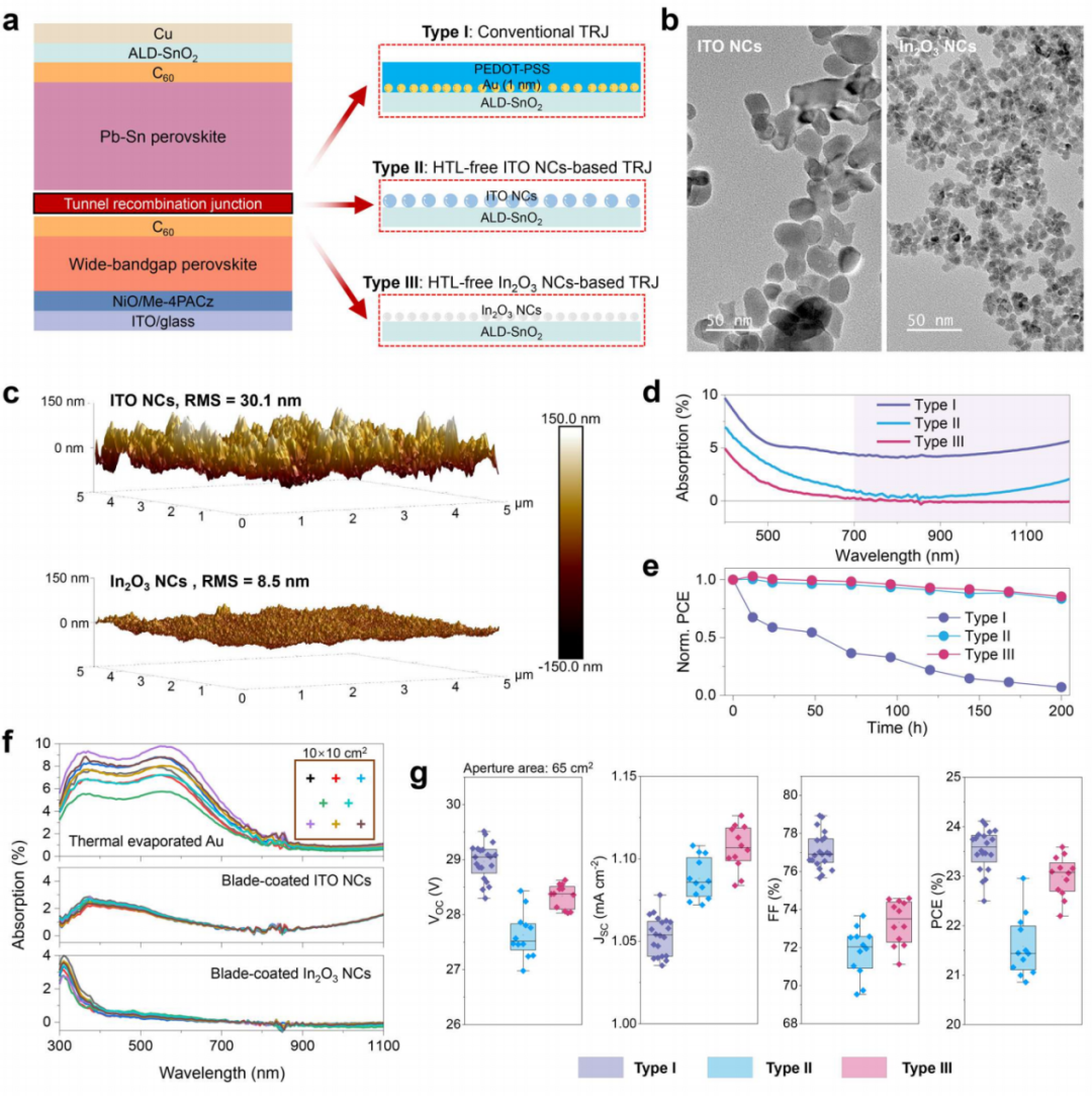
The work proposes a solution-processed alternative: a new TRJ (Type III) constructed from surface-engineered indium oxide nanocrystals (In₂O₃ NCs). It is systematically compared against the conventional Au/PEDOT:PSS Type I structure and a Type II structure based on commercial ITO nanocrystals.
Structure and interface characteristics
The self-synthesized In₂O₃ NCs have a much smaller particle size than commercial ITO NCs, forming a smoother buried interface and effectively lowering contact defect density. Electrical tests show the Type III structure exhibits ideal ohmic contact behavior with no charge transport barrier.
Optical and thermal stability
Optical characterization shows that PEDOT:PSS in Type I causes severe parasitic absorption loss, whereas the In₂O₃ NC film is highly optically transparent. Under 85°C accelerated thermal aging, Type I module efficiency dropped to below half its initial value within 50 hours, while the NC-based Type II and Type III retained about 75% of initial efficiency after 200 hours. On a 10×10 cm² substrate, blade-coated NC films showed far more uniform optical absorption than thin thermally evaporated Au films, fully demonstrating the inherent advantage of solution-processed nanocrystals in scalable manufacturing.
Optimizing Large-Area Perovskite Film Fabrication
With the TRJ's optical loss and instability resolved, uniform fabrication of large-area Pb-Sn perovskite films became the next technical barrier. Conventional DMF/DMSO solvent systems have high boiling points and slow volatility, so their nucleation kinetics lag during high-speed blade coating, making it hard to form uniform films on large substrates.
To solve this, the team developed a binary solvent system based on 2-methoxyethanol (2-Me) and tetrahydrofuran (THF). With its low boiling point and high vapor pressure, this system rapidly reaches critical supersaturation and markedly accelerates nucleation. Using it, the Pb-Sn perovskite blade-coating speed was raised from 5 mm/s in the traditional DMF system all the way to 30 mm/s, delivering highly uniform photoluminescence (PL) intensity and excellent device consistency on 10×10 cm² and larger substrates. This successfully cracked the crystallization-kinetics challenge of large-area coating and achieved a preliminary 17.5% efficiency validation over a 65 cm² aperture area.
Surface Ligand Engineering and Energy-Level Matching
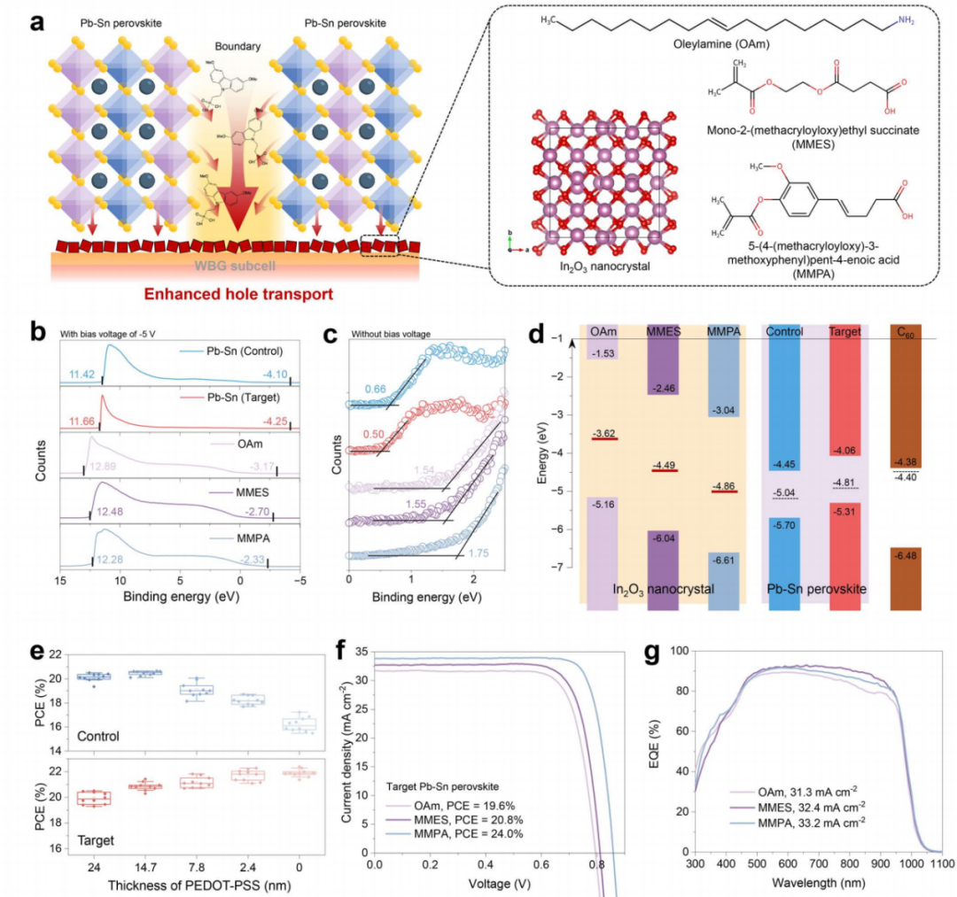
After removing PEDOT:PSS, optical losses fell, but open-circuit voltage (VOC) and fill factor (FF) declined, attributed to increased interfacial transport barriers and non-radiative recombination between the perovskite and the NC layer. To address this, the study implemented a dual synergistic optimization strategy:
Surface ligand engineering to tune energy levels
Through ligand exchange, MMES and MMPA were used to modify the surface of the In₂O₃ NCs. UV photoelectron spectroscopy (UPS) showed that MMPA-modified In₂O₃ NCs achieve favorable interfacial band bending with the target perovskite film (upward bending of about 50 meV), significantly promoting hole extraction, whereas OAm or MMES modification caused downward bending and a transport barrier. Space-charge-limited current (SCLC) tests ruled out any ligand interference on mobility itself, confirming that the performance gain mainly stems from optimized energy-level alignment.
Bulk doping with phosphonic-acid hole-selective material (HSM)
The team doped phosphonic-acid HSMs such as MeO-2PACz directly into the Pb-Sn perovskite precursor (optimized at 0.2 mol%) rather than limiting them to interface modification. This bulk doping strategy avoids the problem of uneven SAM coverage over large areas. UPS showed that after HSM doping the perovskite work function shifted from 5.04 eV to 4.81 eV, the valence band maximum moved up, and the n-type character weakened, better matching the energy levels of the In₂O₃ NCs. The resulting HTL-free single-junction Pb-Sn cell reached 23% efficiency, while a blade-coated device using In₂O₃-MMPA NCs as the hole transport layer (HTL) achieved 24.0% reverse-scan efficiency with a JSC as high as 33.8 mA cm⁻².
Multiple Roles of HSM on the Perovskite Film
The role of HSM goes far beyond charge transport — it profoundly influences film crystallization and defect passivation:
Crystallization control and defect suppression
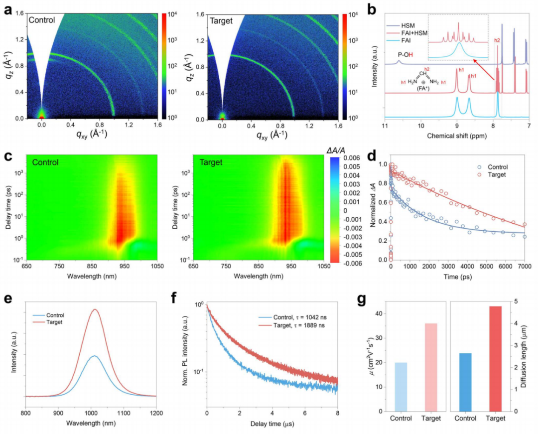
Scanning electron microscopy (SEM) showed that after HSM doping the dendritic impurities originally cutting across grain boundaries in the Pb-Sn film disappeared, grain size grew markedly, and grain boundaries took on a "fused" appearance. GIWAXS and XRD confirmed that HSM effectively suppressed PbI₂ impurity-phase formation. Liquid-state ¹H NMR further revealed that HSM, through preferential deprotonation, consumes free acidic phosphonic groups, thereby preventing their acidic deprotonation of FA⁺ cations and stabilizing the precursor chemistry.
Improved carrier dynamics
Transient absorption spectroscopy (TAS) showed that defect-assisted non-radiative recombination was markedly suppressed after HSM doping. Steady-state PL intensity rose sharply, average PL lifetime extended from 1042 ns to 1889 ns, with especially strong passivation at the bottom interface, effectively reducing charge trapping at the buried interface. OPTP spectroscopy showed the target film's carrier mobility rose from 20 cm² V⁻¹ s⁻¹ to 36 cm² V⁻¹ s⁻¹ and the diffusion length grew from 2.65 μm to 4.78 μm, confirming an all-round improvement in bulk film quality.
Large-Area Module Performance and Stability
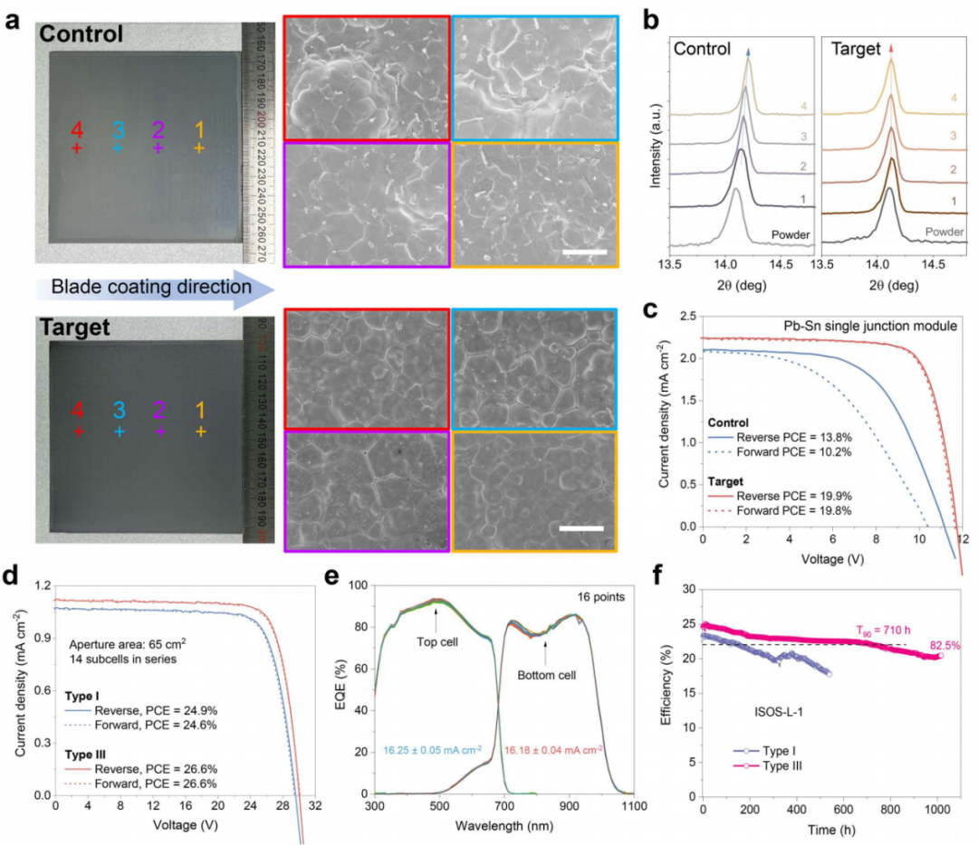
Building on these synergistic strategies, the team fabricated an all-perovskite tandem module with a 65 cm² aperture area (14 sub-cells in series). The champion module using the Type III (In₂O₃-MMPA) TRJ reached 26.6% lab-tested efficiency (reverse scan), with VOC of 30.4 V, JSC of 1.12 mA cm⁻², and FF of 78.2%. Its JET-certified stabilized efficiency reached 26.2%, clearly outperforming the control module using the conventional Type I TRJ (24.8%). After dead-zone optimization, the geometric fill factor reached 96.5%, giving an equivalent active-area efficiency as high as 27.6%. EQE spatial mapping showed that, across 16 different positions, the integrated current densities of the top and bottom sub-cells averaged 16.3 and 16.2 mA cm⁻² respectively — closely matching the J-V results and both breaking the previously reported sub-15 mA cm⁻² module bottleneck.
In terms of reliability, following the IEC 61215:2021 standard, the encapsulated Type III module reached a T90 lifetime (retaining 90% of initial efficiency) of 771 hours under continuous 1-sun MPP tracking, and still held 82.5% efficiency after 1000 hours. In the demanding 85°C/85% RH damp-heat test (ISOS-D-3), the Type III module reached an average T84 lifetime of 1000 hours, while the Type I module had already fallen below 40% efficiency; in the -40°C to 85°C thermal cycling test (ISOS-T-3), the Type III module retained 93% of initial efficiency after 200 cycles. All accelerated aging experiments confirmed that the outstanding stability of Type III stems from completely eliminating the instability factors triggered by PEDOT:PSS.
Through surface-engineered In₂O₃ nanocrystal recombination junctions and synergistic bulk/interface HSM engineering, this work successfully achieved a 26.2% certified efficiency all-perovskite tandem solar module over a 65 cm² aperture area, delivering comprehensive breakthroughs in module size, efficiency, and operational stability. The work strongly demonstrates the commercialization potential of all-perovskite tandem photovoltaic technology. Looking ahead, pushing module area beyond 800 cm² will require synergistic optimization of deposition processes such as slot-die coating together with methods like vacuum-assisted crystallization, to ensure high-quality, uniform fabrication of large-area wide- and narrow-bandgap sub-cells.
Reference and Testing Equipment
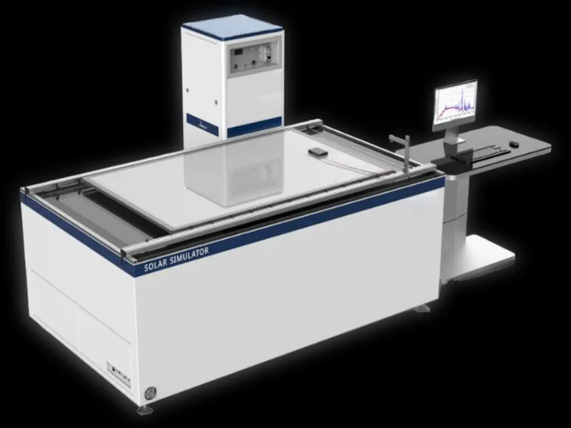
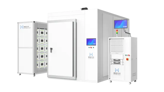
A composite perovskite MPPT tester using an A+AA+ grade LED solar simulator as the aging source provides strong support for perovskite solar cell research through advanced technology and multifunctional design. Such instruments are mainly used for stability testing of finished perovskite single-junction and tandem cells. Because the output characteristics of perovskite cells are easily affected by environmental factors such as light and temperature, the maximum power point fluctuates frequently. An MPPT controller tracks and locks the maximum power point in real time, ensuring the system always operates at optimal power output.
Reference: Nanocrystal-tailored recombination for all-perovskite tandem solar modules
Ooitech's View
Ooitech believes: surface-engineered In₂O₃ nanocrystal recombination junctions paired with HSM bulk/interface engineering have pushed large-area all-perovskite tandem modules to a certified 26.2% efficiency, bringing this technology a decisive step closer to commercialization.