Thinner Silicon Wafers vs. 25-30 Year Module Life: Can
Table of Contents
Quick answer: Silicon wafers are getting thinner, and the question is whether a thinner wafer can still support a 25 to 30 year module life. Two years ago the mainstream thickness sat at 150 µm to 160 µm; current production is moving below that. The motivation is straightforward — thinner wafers mean more wafers per ingot and lower silicon cost per watt, and silicon is the single largest material cost in a module. The risk is mechanical: a thinner wafer is more prone to cracking during cell processing, stringing and lamination, and a micro-crack that does not show at final test can propagate through thermal cycling in the field. Industry capacity in the 600 GW class is being planned around the thinner format, which means the reliability question is being answered at production scale rather than in a laboratory.
PV Module Manufacturing · by Jerry, Ooitech
Introduction
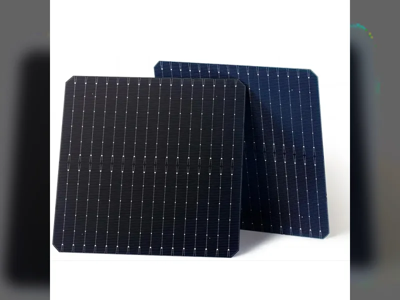
Solar wafers are on a diet in 2026. Two years ago the mainstream thickness still sat at 150-160μm. Now 120-130μm has become the volume-production standard for N-type wafers, and some leading players have pushed 110μm onto their production lines.
So why is the whole industry racing to make wafers thinner? Once wafers keep thinning out, will cells become so fragile they crack at a touch? And can downstream modules still deliver the 25-year, even 30-year, design life? These are real questions the industry and investors both care about.
Why Is the Whole Industry Chasing Thinner Wafers
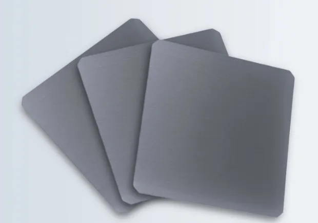
The most direct driver behind wafer thinning is cost reduction, saving precious polysilicon.
Every 10μm cut from wafer thickness lowers silicon consumption per watt by roughly 7%. After deducting the extra non-silicon costs added in cutting and cell steps, the all-in cost per wafer drops by about 0.03-0.04 yuan. Going from 160μm to 130μm saves nearly one jiao per wafer. On a global annual installation of 600GW, that adds up to tens of billions of yuan saved across the industry every year.
Right now polysilicon accounts for 9%-14% of total module cost. Its weight is far below what it was during the polysilicon bull run, but thinning remains the most efficient way to directly cut silicon consumption.
Beyond saving money, thin wafers bring an electrical bonus. The thinner the wafer, the shorter the transport path for photo-generated carriers, so bulk recombination loss falls and cell efficiency ticks up slightly. It pairs even better with TOPCon and HJT.
But different cell routes tolerate thinning very differently. HJT is a low-temperature process with no high-temperature doping step, so it is naturally suited to thin wafers and can go down to 100-110μm. TOPCon has to go through a high-temperature polysilicon deposition step, and too-thin wafers warp easily, hurting yield. That is why TOPCon volume production mostly stays conservative in the 125-135μm range.
How to Control Quality After Thinning, and How Modules Honor Their Warranty
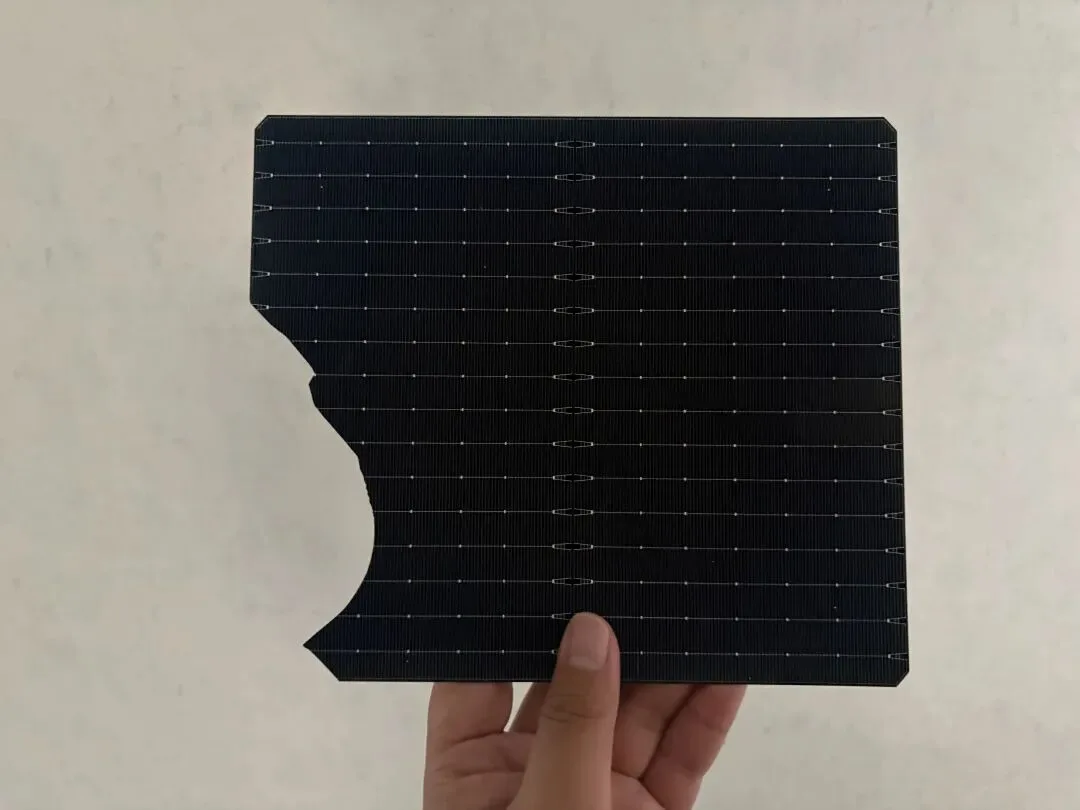
Monocrystalline silicon is a brittle semiconductor material by nature. As thickness drops, the wafer's ability to resist bending and stress falls noticeably. Thin-wafer cells will not shatter at a touch, but the odds of micro-cracks rise clearly. The risk runs across the whole chain: slicing, cell manufacturing, module packaging, logistics, on-site installation, and long-term plant operation.
During wafer cutting and cell production, thin wafers take mechanical squeezing and thermal shock more easily. Texturing, diffusion, printing and soldering can all leave micro-cracks invisible to the naked eye. On TOPCon lines especially, wafer warpage directly causes transport breakage and alignment errors, dragging down whole-line yield.
At the module packaging step, pressure and temperature swings in lamination further amplify internal wafer stress and trigger native micro-cracks. And defects don't all show up at the factory gate. Later shipping jolts, on-site knocks during construction, then the day-in day-out day-night temperature cycling once the plant runs, keep applying stress through thermal expansion and contraction. Fine micro-cracks slowly spread. After two or three years of operation, some micro-cracks turn into visible hidden cracks, breaking the internal current path of the cell, causing abnormal power decline, and in extreme cases triggering hot-spot risk.
Thin wafers themselves don't directly shorten module life. What really threatens the 25-30 year lifecycle is the micro-crack defect that no inspection caught. If the whole flow can keep hidden cracks at a very low level, thin-wafer modules can still hit long-life targets. But if process iteration across the supply chain can't keep pace with the thinning push, defects buried at the manufacturing stage will surface and fail in the middle-to-late years of plant operation. Thinning is essentially a higher bar on the wafer-cell-module manufacturing chain as a whole.
Wafer Cutting: Fine Tungsten Wire Cuts Native Damage
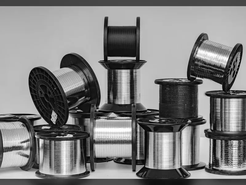
The industry has already widely adopted high tensile strength tungsten diamond wire, replacing traditional carbon-steel diamond wire. Standard thin-wafer lines run wire diameters of 24μm and below. For 110-120μm ultra-thin wafers, even finer 20-22μm ultra-fine tungsten wire is used. The finer the wire, the narrower the kerf, the thinner the damaged layer on the wafer surface, and the fewer surface micro-cracks. That cuts the native micro-cracks a wafer carries out of the factory right at the source.
Cell Manufacturing: Refine the Process, Reduce Impact Cracks
Control focuses on a few key steps. Wet processes slow the water flow and basket swing to reduce knocks and friction. Transport uses flexible mechanisms to lower vacuum suction and motion impact. High-temperature steps slow ramp-up and cool-down rates to suppress warpage and thermal stress. Printing lowers squeegee pressure. Sintering optimizes the temperature-zone curve to avoid hot-cold shock. Each step is paired with PL inspection to screen out micro-cracks and warped bad wafers early, cutting breakage and hidden-crack risk.
Module Manufacturing: Soldering Is Key, Lamination Needs Tuning
When stringing cells, use staged gradient heating and tightly control thermal shock. Use fine, soft ribbon to spread out solder-point stress and reduce single-point squeezing pressure on thin wafers. Tune equipment pressing-pin force to avoid hard-press damage to cells. Choose low-hardness soft ribbon to reduce the pull between ribbon and wafer deformation during thermal cycling. After soldering, add EL inspection to screen out solder-induced micro-cracks early, so they don't pass into lamination.
At lamination, you can try to slow vacuum pumping and ramp rates to soften the pressure shock, while optimizing the temperature-zone curve to avoid internal thermal stress from fast heating and cooling.
Summary
Wafer thinning is a settled industry trend, and there's no point flatly rejecting it. While the whole chain rides thinning for lower cost and better output, the wafer, cell and module steps have to upgrade equipment and process together, tightly control mechanical and thermal stress, guard against hidden cracks and breakage, and strengthen full-flow inspection. That is how you hold the line on long-term module quality and reliability while still cutting cost.
Ooitech's View
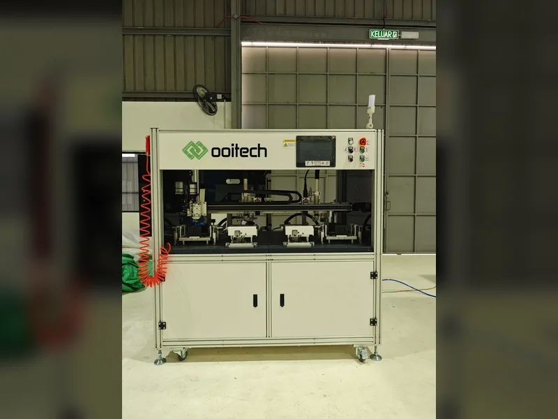
Thinning is really a stress-management problem that lands hardest at the module line, and that's where equipment choices decide whether those buried micro-cracks ever show up. On our side, stringers with segmented gradient soldering and soft-ribbon handling, plus EL screening before lamination, are exactly the guardrails that keep 110-130μm cells from turning into field failures five years down the road. The physics of thin wafers is set, but the yield is won or lost in how gently your line handles them. If you want to see how a real MBB module line runs these steps, the Ooitech YouTube channel at www.youtube.com/ooitech is worth a look.