Editorial responsibility for this article rests with Wuhan Ooi Photoelectric Technology Co., Ltd. Written and reviewed by the Ooitech editorial team. See our editorial policy for how we write, where AI tools are used, and how to request a correction.
Bypass Diode Selection: Six Numbers and Two Words
Table of Contents
Quick answer: A bypass diode datasheet for a PV junction box fits on one page: VRRM, IF, VF, IR, Tj and Rth, plus a two-word process name such as 150 trench. Six numbers read like a menu of sizes. They are not. VF decides how many watts the part dumps into a sealed, potted box on the back of a module. IR decides what happens to that box at 125 °C, because leakage climbs with temperature while the box still sheds only what its surfaces allow. The two pull against each other, so every selection is a trade. And the current on the page is a chip figure, measured under heat sinking that a junction box does not offer. Public box datasheets pair a 50 A, 45 V diode with a 30 A assembly rating. Read the six numbers, then read the box they go into.
Fifteen amps of string current passes a bypass diode every sunny hour without touching it. On the afternoon a leaf lands, the same part carries the whole substring and turns that current into heat.
What the part does when nothing is wrong
Every cell sits in series with every other cell, so the string current has one path through the whole module. Shade one cell and it stops being a source. The rest of the string keeps pushing current through it, the voltage across that cell reverses, and the shaded cell turns the current into local heat. A diode connected across each substring gives the current a lower-resistance route around the shaded section. Conventional modules carry three of them, and each covers roughly one third of the cells.
In normal operation nothing happens. The diode sits at reverse voltage across its substring, blocks, and leaks microamps. The voltage it has to block is the open-circuit voltage of one substring, which on a modern module is only in the teens of volts. What a shaded cell then does to itself is a separate subject, covered in reverse bias and hot-spot formation.
Two corrections are worth keeping. A bypass diode is not a blocking diode: that part sits in series to stop reverse current, a different job. And a bypass diode does not remove hot-spot risk. It caps reverse voltage at one substring, which caps the heat, rather than zeroing it.
Where the heat comes from
A conducting diode charges a toll, and the toll is roughly P ≈ VF × I. Silicon PN junctions charge 0.7 to 1 V. Schottky junctions charge 0.4 to 0.5 V. That fraction of a volt is the whole reason almost every PV bypass diode is a Schottky.
Take a module running 15 A. At 0.45 V the diode burns about 7 W while it is bypassing. Push the same 15 A through a PN junction at 0.7 to 1 V and the figure is 10.5 to 15 W. Neither number sounds dramatic until you place it: a sealed box, filled with potting compound, bonded to the back of a module already sitting at 70 to 80 °C in the field, with no airflow to speak of.
The temperature the chip reaches is that wattage multiplied by the thermal resistance from junction to the outside world, plus ambient. The datasheet hands you the wattage. The box hands you the resistance. That is why an excellent datasheet can still fail in a specific assembly.
Six numbers, and what each one is for
A photovoltaic bypass diode datasheet is short. Six lines carry almost all of the decision.
| Parameter | What it states | What to check |
|---|---|---|
| VRRM | Reverse voltage the part blocks while off | 45 V and 50 V are common. One substring’s open-circuit voltage is only in the teens of volts, so margin here is generous and rarely the constraint. |
| IF | Rated continuous forward current | Parts are commonly marked 30, 40 or 50 A. That is a chip figure, not the rating of the box it is mounted in. |
| VF | Forward voltage drop while conducting | Lower is better, and it maps directly to watts. Ask for VF at the current and temperature your product will run, not at 25 °C only. |
| IR | Reverse leakage while blocking | Small at room temperature, multiplied at high temperature. It is the input to thermal runaway, so ask for the curve rather than the 25 °C point. |
| Tj | Maximum junction temperature | PV Schottky parts usually specify 200 °C or below. It is the limit the bypass diode test measures against. |
| Rth | Thermal resistance, junction outward | Set by package and box structure. Smaller is better, and it is the one number a diode supplier cannot give you for your housing. |
Four lines describe the part. Two describe a system. VRRM is nearly free margin in a substring application, Tj is a limit rather than a target, and Rth leaves the supplier’s control the moment the diode is potted into your box. The pair that actually decides the selection is VF and IR, because they move in opposite directions and both of them end at temperature.
Why 30 A on the diode is not 30 A in the box
Diode current ratings are quoted under heat-sinking conditions that a junction box does not provide. Once the part is soldered to a copper pad, covered with potting compound and clamped against a backsheet running at 70 to 80 °C, the current it carries continuously is lower than the label. The derating is not an admission of a bad part. It is the difference between a chip on a heatsink and a chip in a plastic box.
When we laminate module stacks designed for backsheet temperatures of 70 to 80 °C, we control chamber pressure and temperature profiles to keep the junction box bonding area flat and uniform.
Public junction box datasheets show the arithmetic in plain sight: it is common to find a nominal 50 A, 45 V diode specified inside an assembly rated at 30 A. The diode is not mislabeled and the box is not being conservative. The two numbers answer different questions, and only the second is a promise about the assembly you buy. Negotiate on the assembly rating, which is the number the thermal tests exercise.
Ratings in mass production cluster at 25 A and 30 A, with 35 A and 40 A for 210 mm and high-power bifacial products. When a quotation says 30 A, the useful follow-up is 30 A at what ambient, with what potting, and whether that figure survives the tests in the next section.
Two tests the number has to survive
Both IEC tests are junction temperature measurements in disguise, and both run on an assembly rather than on a component.
The bypass diode thermal test, IEC 61215-2 MQT 18.1, heats the module to 75 °C, drives the module short-circuit current through the diode and measures the junction, then repeats at 1.25 × Isc for one hour, and the junction has to stay below its rated maximum with the diode still working afterwards.
Before running modules through the 75 °C thermal test at 1.25 × Isc for one hour, we verify that our lamination recipe cures the encapsulant evenly around the copper busbar exits without voids.
The thermal runaway test, IEC 62979, targets Schottky parts specifically: heat the diode with forward current until it is thoroughly hot, switch to reverse voltage, and watch whether it cools itself down.
The runaway loop is why IR deserves more attention than its microamp value suggests. Hotter junction, more leakage, more reverse dissipation, hotter junction. A part with a comfortable forward drop and a careless leakage curve can pass a forward test and fail this one. It is one item on a longer list, which is why the reliability test list is worth reading before you accept a diode qualification report.
The number before the word: what 130, 150 and 180 mean
Buyers and process engineers discuss diodes in a shorthand that never appears on a datasheet. This box uses a 150 trench. Can we drop to a 130. Two pieces of information are packed into that. The number is the chip edge in mil. The word is how the chip is built. One mil is one thousandth of an inch, or 0.0254 mm.
The chips are square, so 150 means an edge of 150 mil, or 3.81 mm. The rest is arithmetic that is easy to get wrong in a meeting.
| Chip | Edge (mm) | Area (mm²) | Relative area | Relative edge |
|---|---|---|---|---|
| 130 | 3.30 | 10.9 | 1.00 | 1.00 |
| 150 | 3.81 | 14.5 | 1.33 | 1.15 |
| 180 | 4.57 | 20.9 | 1.92 | 1.38 |
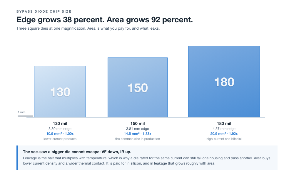
Going from 130 to 180 grows the edge by 38 % and the area by 92 %, because area scales with the square of the edge. For a given current the current density falls by the same factor the area rises, so VF falls, and the die spreads its heat over a wider contact patch against the copper. The price rises with area, because silicon is sold by area, and leakage rises roughly in proportion, which is what buyers forget when they ask for one size up.
Three dies at one magnification. From 130 to 180 mil the edge grows 38 percent and the area grows 92 percent. Drawn from the dimensions in the reference article below; the relative edge figures are our arithmetic.
The drawing above makes the step look smaller than it is, which is the point. So the size question is not which one is safer. It is how much margin your housing has and what that margin costs. A 130 mil die on thick copper with good potting can run cooler than a 180 mil die on thin copper, because Rth is set by more than the chip. Module current sets the floor on size, but the floor is a starting point rather than a rule.
Planar against trench: two ways to hold the same field
The second word is the chip structure, and it exists to solve one problem. A Schottky barrier is a metal-silicon interface, and reverse voltage across that interface is where leakage comes from.
Planar: the see-saw is the design
A planar Schottky puts a flat barrier on the surface. It is simple, mature and cheap. Its difficulty is a see-saw: push VF down and IR climbs by a multiple, hold IR down and VF will not come down. The trade is set by the barrier and the drift region, with little room left inside it.
Trench: blocking the field instead of the current
A trench Schottky etches a row of micrometer-scale grooves into the silicon, grows an oxide layer on the walls and fills them. Under reverse bias the adjacent trenches pinch off the silicon between them, and the oxide stands between the metal-silicon interface and the strong field. Leakage drops. The area that was being spent on holding the field can then be spent on conduction, so VF can be pushed lower at the same die size. The process costs more.
| Dimension | Planar | Trench |
|---|---|---|
| Forward voltage drop | Higher | Lower |
| Leakage at high temperature | Larger | Smaller |
| Margin against thermal runaway | Adequate | Better |
| Process and cost | Simple, cheaper | More complex, more expensive |
| Die area for the same current | Larger | Can be smaller |
One size down in trench is a claim you have to test
The two halves combine directly. 150 trench is a 150 mil trench chip; 180 planar is a 180 mil planar chip. Because the trench part does more per square millimeter, the industry commonly matches a trench one size smaller against a planar one size larger, and on paper the pair looks equivalent.
Whether it is equivalent in your box is a different question, because the trench advantage is mostly an advantage at temperature, and your potting, your copper and your backsheet set the temperature. Substitution gets decided by measured junction temperature and a thermal runaway result in the actual assembly, not by mil against mil.
Reading the part number, the package and the box
Part numbers follow a loose convention. 3045, 4045 and 5045 are the familiar ones: the first two digits are the current in amps, the last two the voltage in volts, so 5045 is 50 A at 45 V. It is common rather than universal, so match it against the marking on the part you buy.
Three package styles appear in boxes. Axial leaded parts have largely left mainstream modules. SMD parts and module diodes share what is left, and the module diode is the interesting one: the chip is soldered directly to the copper busbar inside the box and encapsulated, which shortens the thermal path and explains why it dominates high-current products. The Chinese group standard T/CPIA 0052-2023 exists specifically for module diodes, which tells you how far the category has moved.
One-piece and two-part housings are the other variable. One-piece puts three diodes in one box. Two-part splits them into three small boxes with one diode each. Two-part is now the mainstream, because three heat sources spread over three locations run cooler than three sources in one housing, and the layout suits half-cut modules. The reasoning sits in the note on two-part junction boxes.
The last two production steps decide whether the datasheet number survives contact with the product. The diode is welded or soldered to the busbar, then the box is filled with a thermal potting compound that keeps water out and moves heat. Both are equipment decisions with process windows: the junction box welding step and AB potting. A cold or voided joint adds thermal resistance where the die cannot afford it, the failure mode in the cold solder joint note.
Where these numbers come from
The source is a Chinese-language engineering explainer on bypass diodes in PV junction boxes, written for module process and material engineers. Almost every number in this article comes from it: the three diodes per conventional module and the one-third coverage, the 15 A module current, 0.7 to 1 V for a PN junction and 0.4 to 0.5 V for a Schottky, the 7 W figure, the 45 V and 50 V reverse ratings, the 30, 40 and 50 A chip ratings, the 200 °C junction limit, the 50 A, 45 V diode inside a 30 A assembly, the 75 °C and 1.25 × Isc conditions with a one-hour hold, 1 mil = 0.0254 mm, the three die dimensions and their 10.9, 14.5 and 20.9 mm² areas with relative areas of 1.00, 1.33 and 1.92, the planar and trench descriptions, the part-number convention, the three package styles, and the 25 A to 40 A assembly ratings now in production.
Two things here are our arithmetic rather than the source’s table. The 10.5 to 15 W figure is 15 A multiplied by the stated 0.7 to 1 V range. The relative edge column, 1.00, 1.15 and 1.38, is the edge dimensions divided by 3.30 mm. That larger module currents bring larger dies is the source’s statement, not a measured distribution.
The source also says its figures are typical magnitudes, so treat them as such. A datasheet, a potting specification and a measured junction temperature outrank every number here.
Frequently asked questions
Q: Is a 30 A bypass diode fine for a 30 A junction box?
Not by itself. The 30 A on the diode is a chip rating quoted under heat-sinking conditions; the 30 A on the box is an assembly rating that already accounts for potting, copper and housing. Public box datasheets routinely pair a 50 A, 45 V diode with a 30 A assembly rating. Match the assembly rating, then check the junction temperature the assembly reaches.
Q: Why not use a PN diode, since it is cheaper?
Because the forward drop is 0.7 to 1 V instead of 0.4 to 0.5 V, and that difference is wattage. At 15 A a PN part dissipates 10.5 to 15 W against about 7 W for a Schottky, in a sealed box. The box, not the diode, becomes the limit.
Q: What does 150 trench mean in a quotation?
A trench-structure Schottky chip with an edge of 150 mil, or 3.81 mm. The number is the die size and the word is the process. Neither tells you the assembly rating, the potting compound or the measured junction temperature, so ask for those separately.
Q: Can a 150 mil trench chip replace a 180 mil planar one?
The industry often pairs them, because a trench die does more per square millimeter. It is a claim about your housing, though. The replacement holds if the measured junction temperature and the thermal runaway result in your assembly are acceptable, which is a test rather than a comparison of numbers.
Q: Which number predicts trouble first, VF or IR?
IR at temperature, in most field failures, because it feeds the runaway loop. VF decides the steady heat load while the diode is bypassing. A part with a good VF and a poorly controlled leakage curve can pass a forward test and fail a reverse one.
Q: Does one bypass diode protect the whole module?
No. Conventional modules carry three, each across one substring, so a shaded cell takes down about one third of the module rather than all of it. The diode caps reverse voltage at one substring, and the heat with it. It does not eliminate hot-spot risk.
Q: How is a bypass diode different from a blocking diode?
A bypass diode sits in parallel with a substring and conducts only when that substring is shaded. A blocking diode sits in series with the string and stops reverse current from flowing back into the array. They protect against different events and are not interchangeable.
Q: Does a bigger chip always run cooler?
It lowers current density and spreads heat over a wider contact patch. But the junction temperature is watts times thermal resistance, and the die attach, the copper and the potting dominate that resistance. A large die on thin copper can run hotter than a smaller die with a better path out.
Final thoughts
The six numbers and the two words are not a menu you choose from. They are the answer to a thermal problem that your box, your potting and your backsheet have already solved or already failed. Fix the assembly rating first, measure the junction temperature in the housing you will actually ship, and let the die size and the process name follow from that. A bigger chip buys margin. It does not buy a cooler box.
OOITech builds single and double chamber solar panel laminator machines with oil-heated or electric platens to deliver uniform thermal control across each panel. Send your drawings, a module stack, or samples for evaluation, and we will help you verify thermal cycles suited for your junction box assembly.