Why Does Fill Factor Reveal Solar Cell Mass-Production
Table of Contents
Quick answer: Fill factor is the ratio of a cell's maximum power to the product of its open-circuit voltage and short-circuit current, and it is the parameter that reveals mass-production defects before the other two do. A cell can hold its voltage and its current while its fill factor slips, because fill factor is where series resistance and shunt losses appear. Series resistance comes from the metallisation, the contacts and the ribbon joints; shunt losses come from defects that let current bypass the junction. In a production environment with capacity in the 150 GW to 200 GW range, a fill-factor drift across a batch is the earliest signal that a firing step near 800 °C or a later process stage near 200 °C has moved out of window. That is why fill factor is monitored continuously rather than at final test alone.
PV Module Manufacturing · by Jerry, Ooitech
Why Does Fill Factor Reveal Solar Cell Mass-Production Defects First?
Introduction: Fill factor is not an isolated parameter. It compresses contact resistance, leakage, paste formulation, screen printing, firing, and the LECO process window into a single I-V curve.
Efficiency Shows the Result, While FF Reveals What Is Happening on the Production Line
The photovoltaic industry has expanded quickly under the global energy transition. Global PV module production capacity has already crossed 200 GW, with annual output remaining above 150 GW. At the same time, PERC technology has entered the later stage of its lifecycle. Mass-production conversion efficiency has risen to 23.5% and is moving with difficulty toward a theoretical ceiling of around 24%. Further gains are becoming much harder.
From a manufacturing-cost perspective, the non-silicon cost of PERC cells has been compressed to about RMB 0.2 per watt, leaving limited room for further reductions. The industry has therefore shifted toward high-efficiency N-type technologies such as TOPCon, heterojunction technology, or HJT, and back-contact cells. The goal is to open new profit space through higher efficiency and stronger project bankability.
Conversion efficiency is clearly important when evaluating a generation of solar cell technology. On a real mass-production line, however, open-circuit voltage, or Voc, and short-circuit current, or Isc, often stabilize within relatively narrow ranges. At that point, fill factor becomes a decisive indicator of final production yield and a sensitive signal of small process fluctuations.
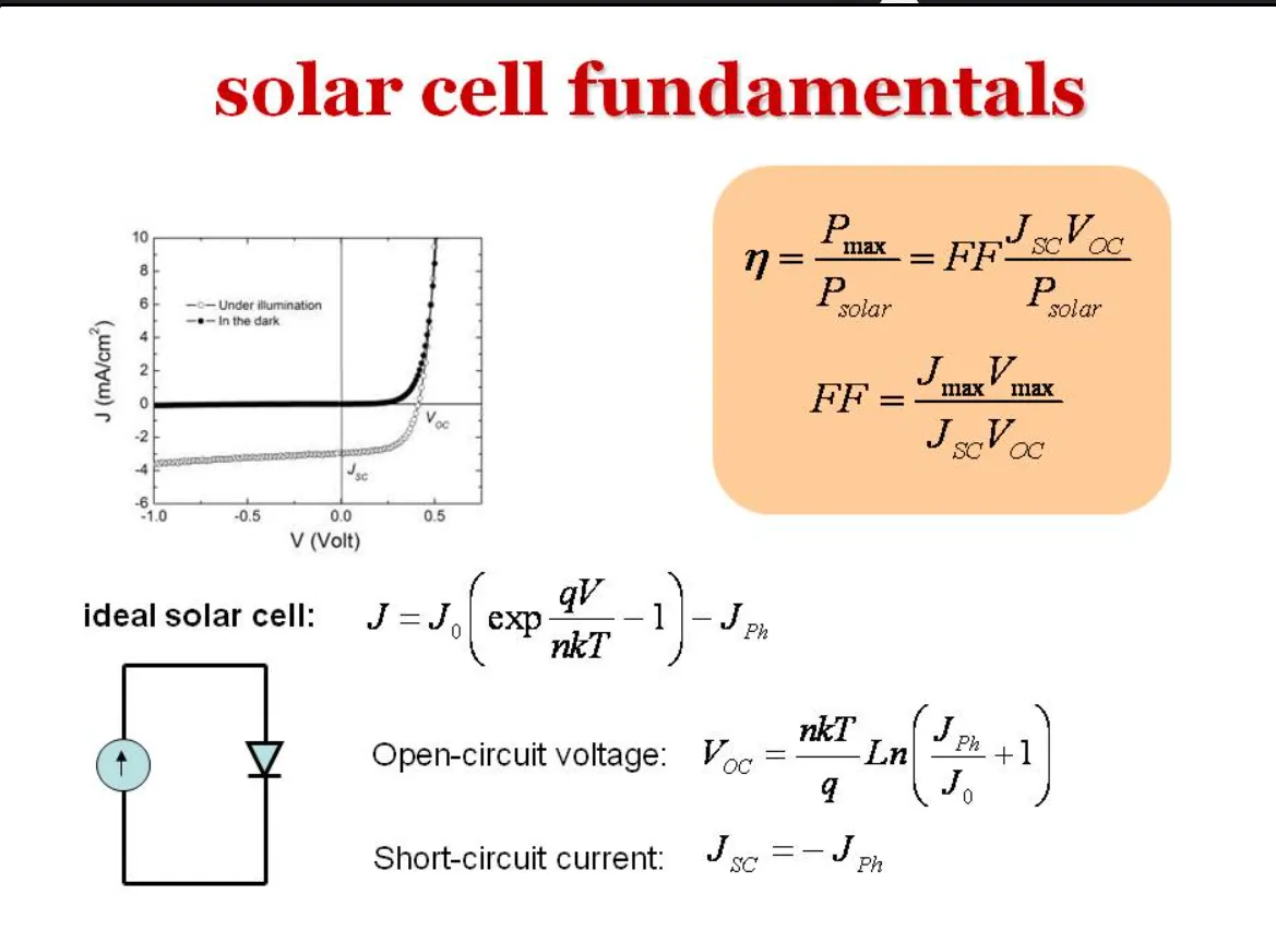
Geometrically, fill factor measures the squareness of a solar cell's I-V characteristic curve. It is the ratio between the actual maximum-power rectangle and the theoretical rectangle formed by Voc and Isc. The value is always below 1. Under ideal conditions, the maximum FF of a gallium arsenide solar cell may approach 0.89. The theoretical limit for a typical commercial crystalline-silicon solar cell is approximately 0.83 to 0.85.
A production line is not an ideal model. Poor metallization contact, etching-related leakage, an unbalanced paste formulation, or a shifted firing window can all disturb microscopic contact interfaces. These defects are highly sensitive to heat accumulation. They eventually appear as sharp variations in parasitic resistance and are often exposed first through a decline in FF.
Formula: Relationship Between Conversion Efficiency and FF
η = Pmax / Pin = (Voc × Isc × FF) / Pin
Meaning: When Voc and Isc remain relatively stable, a small FF fluctuation passes directly into the final conversion efficiency.
Formula: Definition of Fill Factor
FF = Pmax / (Voc × Isc) = (Vmp × Imp) / (Voc × Isc)
Meaning: FF measures the squareness of the I-V curve. In practical terms, it shows how effectively a cell converts its theoretical electrical output into actual maximum power.
The Physical Core of FF: The Pull Between Rs and Rsh
To understand why FF is so sensitive to manufacturing conditions, it is necessary to return to the equivalent-circuit model of a solar cell. Photogenerated carriers drift and diffuse through the silicon body before being collected by the external circuit. Energy losses are unavoidable during this process.
At the macroscopic electrical level, these losses are represented by parasitic resistance. The two main components are series resistance, Rs, and shunt resistance, Rsh.
Series resistance represents all forward physical resistance encountered when current flows toward the external load. It is the combined result of silicon wafer bulk resistance, contact resistance between the front and rear electrodes and the silicon, lateral emitter transport resistance, finger and busbar resistance, and, at the module level, interconnection ribbon resistance.
Among these contributors, metal-semiconductor contact resistance and variations in emitter doping concentration and junction depth are some of the least stable variables in mass production. They are also among the most likely causes of a sharp Rs increase. Series resistance has a strong negative correlation with cell fill factor.
On the I-V curve, when Rs increases, the slope of the forward-bias region near Voc decreases and the curve becomes flatter. At the macroscopic level, higher series resistance reduces maximum output power and pulls down FF.
Shunt resistance reflects the level of internal electrical leakage. Ideally, Rsh should approach infinity, leaving no bypass path for photogenerated carriers. In actual manufacturing, edge leakage, crystal dislocations, and metal paste penetrating the PN junction can create unintended current paths.
A lower Rsh means more internal leakage current. This shunting effect reduces the current passing through the functional PN junction and lowers the operating voltage. The problem becomes more visible under low irradiance because the photogenerated current is already weak, making leakage a larger part of the total current.
Formula: Solar Cell Equation Including Parasitic Resistance
I = IL - I0 × { exp[q(V + I×Rs)/(n k T)] - 1 } - (V + I×Rs) / Rsh
Meaning: Rs obstructs current output, while Rsh creates a leakage path. Both reduce FF.
Formula: Maximum Power Point Condition
d(I×V) / dV = 0
Meaning: The point at which power reaches its maximum on the I-V curve is the source of the Pmax value used in production testing.
Formula: Normalized Shunt Resistance
RCH = Voc / Isc; rsh = Rsh / RCH
Meaning: Normalization with the characteristic resistance RCH allows cells of different sizes and current classes to be compared on the same scale.
Formula: Approximate Effect of Shunt Resistance on FF
FFsh ≈ FF0 × (1 - 1 / rsh)
Meaning: The lower the Rsh, the more severe the leakage and the greater the resulting FF loss.
Which Production Problems Correspond to Rs and Rsh?
From an engineering perspective, FF is valuable not because it simply says that efficiency has fallen. It helps engineers determine why efficiency has fallen. Series resistance and shunt resistance affect different regions of the I-V curve, so they can point toward different manufacturing defects.
Formula: Thermal Loss Caused by Series Resistance
Ploss ≈ I² × Rs
Meaning: Under high-current or high-irradiance conditions, the power loss caused by Rs increases with the square of the current.
| Parasitic resistance condition | Change in the I-V curve | Macroscopic effect | Likely production-line causes |
|---|---|---|---|
| Series resistance, Rs, increases | The slope in the forward-bias region near Voc decreases | FF falls, thermal loss becomes greater under high irradiance, and Isc may decline slightly | Poor front or rear electrode contact, high paste bulk resistivity, broken fingers, or insufficient firing |
| Shunt resistance, Rsh, decreases | The slope near Isc and in the reverse-bias region increases | FF falls, leakage lowers Voc, and low-light performance deteriorates more sharply | Incomplete edge isolation, PN-junction penetration caused by overfiring, crystal defects, or pinholes in the passivation film |
Poor Contact: The Achilles' Heel of Metallization

In the process flow from silicon wafer to finished cell, screen printing and metallization firing are critical stages that determine electrical performance. Screen printing is mature and cost-effective, but its physical contact mechanism can create both series-resistance and shunt-resistance problems.
Modern high-efficiency cells commonly use rear dielectric passivation and local metal-contact structures to reduce the surface recombination rate of rear-side carriers. Because an insulating dielectric layer sits between the metal and silicon body, local contact must be formed through laser opening or paste-assisted etching. If the opening quality is poor or alloying is insufficient, the metal and semiconductor cannot form a reliable ohmic contact.
A study of cells with screen-printed local rear-electrode contacts showed that poor contact caused series resistance to rise to 21.34 mΩ. Conversion efficiency reached only 8.95%, far below the 17.44% level of a conventional aluminum back-surface-field cell.
The researchers attempted to recover FF by adjusting the doping level of the rear aluminum paste. As the aluminum content increased, alloying depth improved and series resistance decreased. When the aluminum content reached a critical level of 60%, Rs was reduced by 11 mΩ compared with the undoped condition. This raised conversion efficiency by an absolute 2.59 percentage points.
Once the aluminum content became too high, however, excess aluminum disrupted the conductive network in the contact region. Series resistance then began to rise again.
QFLS: Separating Material Defects from Manufacturing Defects
When a production line shows a widespread reduction in FF, one of the hardest questions is whether the loss comes from excessive non-radiative recombination inside the material or from parasitic resistance introduced during screen printing and firing.
Quasi-Fermi level splitting, or QFLS, is an important diagnostic tool in this situation. In physical terms, QFLS determines the theoretical voltage limit of a photovoltaic device when no external charge extraction occurs. The difference between QFLS and the radiative limit directly reveals non-radiative recombination losses caused by material defects or impurities.
By measuring QFLS optically and combining it with contactless pseudo J-V analysis, researchers can remove the influence of series resistance from the external electrical measurement.
If the measured FF is far below the pseudo fill factor derived from QFLS, the loss can usually be linked to poor metallization contact or broken fingers. If the pseudo fill factor is already low, non-radiative recombination is likely out of control, pointing toward an intrinsic problem in wafer quality or interface passivation.
HJT Low-Temperature Silver Paste: Building a Conductive Network Below 200°C
As N-type technologies expand, HJT and BC cells place stricter requirements on metallization quality. FF has therefore become an important indicator for evaluating innovative conductive pastes.
HJT cells use an amorphous-silicon and crystalline-silicon heterojunction structure. This provides strong passivation, but the structure is highly temperature-sensitive. To prevent crystallization and degradation of the amorphous-silicon films, HJT cells cannot withstand conventional firing temperatures above 800°C. They require low-temperature silver paste with a curing temperature strictly controlled below 200°C.
Low-temperature silver paste works differently from conventional high-temperature paste. High-temperature silver paste relies on glass frit melting at elevated temperatures. The glass frit etches through the antireflection film and promotes the growth of silver crystallites into the silicon, creating a low-resistance ohmic contact.
Low-temperature silver paste depends mainly on silver particles suspended in a polymer resin system. After the solvent evaporates at low temperature, the particles are pressed together to form physical electrical contacts.
This mechanism generally gives low-temperature paste a higher bulk resistivity than high-temperature paste. It can increase the total series resistance of the cell and reduce FF. Paste suppliers are addressing the problem through nanoscale powder engineering. Typical measures include reducing silver content and improving paste fineness and rheology so that a dense conductive network can be formed with lower silver consumption.
| Paste type | Silver content | Curing conditions | Bulk resistivity | Process characteristics |
|---|---|---|---|---|
| Conventional low-temperature silver paste | 35%-55%, or as low as 20%-35% | Conventional settings | Approximately 4-8 μΩ·cm | Fineness of about 6-8 μm and viscosity of approximately 155-165 Pa·s |
| AP-01 series, solvent-containing | 33%-41% | At least 120°C for 6-20 minutes | 4.57-7.62 μΩ·cm | Supports high aspect-ratio printing and very fine line widths |
| AP-02 series, solvent-free | 33%-41% | At least 110°C for 5-15 minutes | 4.31-8.53 μΩ·cm | Suitable for screen openings above 15 μm and printing speeds above 400 mm/s |
BC Cells: FF as an Alarm for Rear-Side Isolation Failure
If the challenge for HJT lies in low-temperature conductivity, the challenge for back-contact cells lies in the microscopic limits of electrode layout.
BC cells eliminate front-side metal grid shading and can therefore push Isc higher. The trade-off is that all positive and negative electrodes must be arranged alternately at very small spacing on the rear surface.
Within this high-density wiring area, a slight screen-printing offset, paste spreading, or a tiny isolation-layer defect may create a physical connection between the positive and negative electrodes. When that happens, Rsh can fall almost to zero.
A microscopic short circuit creates a large shunt current that drains the operating voltage. Voc collapses and FF may fall to zero. Photogenerated carriers created near the front surface must also travel a longer lateral distance before reaching the rear metal collection electrodes. This increases the risk of accumulated bulk and lateral series resistance.
For this reason, FF fluctuation monitoring is one of the most important yield-protection measures on a BC cell production line. Each cell that fails the FF threshold may represent a failure in metallization isolation or carrier-transport design.
The Firing Window: Both Underfiring and Overfiring Are Punished by FF
For TOPCon and PERC cells, high-temperature firing is one of the final critical processes. Silicon wafers with printed metal electrodes pass through a belt furnace with a peak temperature of around 800°C. The glass frit in the metal paste melts through the surface passivation layer and forms an alloyed or direct contact with the underlying silicon or back-surface field. This creates an ohmic contact and reduces series resistance.
The process is a tight balancing act. A temperature that is too low, or a belt speed that is too high, causes underfiring. The glass frit cannot melt sufficiently and may fail to etch through the silicon nitride or tunnel oxide layer. Too few silver crystallites precipitate and penetrate into the silicon. An insulating layer remains between the metal and semiconductor, causing contact resistance to rise sharply. The forward-bias side of the I-V curve flattens, and FF becomes abnormally low.
Excessive temperature causes overfiring. The metal paste becomes too aggressive, and silver crystallites can penetrate a shallow PN junction like spikes. This introduces short circuits and recombination centers. Passivation is damaged, Rsh decreases, and leakage becomes a serious problem.
In EL inspection, lattice damage and passivation failure caused by overfiring often appear as cloudy patterns, watermarks, or furnace-belt marks.
To widen the process window, equipment suppliers have developed firing and light-injection systems. These systems combine a firing furnace with a light-injection chamber. After high-temperature annealing and alloying, the wafer is directly exposed to high-intensity light at a temperature of approximately 150-350°C.
High-intensity photons excite carriers and change the charge state of hydrogen atoms inside the wafer and near its surfaces. This can passivate microscopic thermal defects and dangling bonds created during firing. Test results show that this treatment can reduce EL watermarks and furnace-belt marks while improving both Voc and FF.
LECO: A Non-Equilibrium Route Through the TOPCon Metallization Conflict
During the early expansion of TOPCon, front-side metallization became a major yield bottleneck. To reduce surface recombination, the front side of a TOPCon cell tends to use a shallower emitter with lower doping concentration.
A shallow junction and low doping create a conflict for conventional high-temperature silver paste containing glass frit. If the paste is not fired through sufficiently, contact resistance remains extremely high. If it is fired too aggressively, the shallow junction may be penetrated, creating leakage and driving FF toward zero.
Laser-enhanced contact optimization, or LECO, was developed to address this conflict. LECO uses a non-thermal-equilibrium photoelectric mechanism. Instead of applying destructive global high-temperature heating, it excites charge carriers with a high-intensity laser while applying a reverse bias of around 10 V or higher.
Under the combined effect of strong bias and photogenerated carriers, weak insulating points left unconnected by underfiring undergo localized avalanche breakdown. Free carriers are driven through the metal-semiconductor contact by the electric field, creating local currents of several amperes.
These strong currents generate localized Joule heating at microscopic contact points. This produces micro-firing on a nanosecond-to-microsecond timescale.
LECO changes the TOPCon firing strategy from aggressive global heating to targeted local repair. Paste suppliers can design dedicated LECO-compatible glass frit systems. The conventional belt-firing process can then remain slightly underfired to protect the shallow emitter, while LECO creates localized electrical breakdown at the back end and reduces contact resistance.
Validation results show that cells without LECO may operate close to failure because of excessive contact resistance. After LECO treatment, contact resistance decreases while passivation is retained. FF rises, leading to an absolute conversion-efficiency gain of more than 0.2 percentage points.
LECO still has a process boundary. If the light intensity is too low, contact repair is incomplete. If it is too high, lattice ablation and structural damage may occur.
When the laser intensity reaches a destructive value of 375 MW/cm², FF can fall from 0.84 to 0.65, a decline of about 24%. Voc may decrease from 0.745 V to 0.695 V, while Jsc falls from 41.8 mA/cm² to 40.8 mA/cm².
The microscopic contact network created by LECO also has a degree of non-equilibrium thermal fragility. EL analysis shows that when a LECO-treated cell undergoes a second high-temperature firing cycle, increasing the second firing temperature from 280°C to 680°C can disturb the established micro-conductive paths.
Contact resistance then deteriorates again, FF shrinks significantly, and an initial cell efficiency of 26.35% begins to decline.
FF Is Not Just a Percentage. It Is the Pulse of Production Yield
Looking inside the black box of solar cell manufacturing makes one point clear: fill factor is far more than an abstract percentage shown on a laboratory tester.
At the microscopic level, FF is the final expression of the pull between series resistance and shunt resistance along the carrier-transport path. On a production line, it records the conductivity limits of the metallization paste, the mechanical precision of screen printing, and small shifts in the temperature profile of a belt-firing furnace.
In a new PV cycle where non-silicon costs are already close to the bottom and capital expansion is becoming more demanding, every major high-efficiency technology faces the same basic problem.
HJT must maintain a reliable conductive network within a low-temperature curing limit. BC cells must control leakage between positive and negative electrodes separated by only a microscopic distance. TOPCon relies on firing, light injection, and LECO to repair contact while protecting passivation.
The target is always the same: reduce interface contact resistance without penetrating the PN junction and creating leakage.
For manufacturers, chasing the absolute efficiency value alone is no longer enough. A smarter production system should monitor small FF variations in real time and combine them with non-destructive diagnostic methods such as QFLS and pseudo J-V analysis. That is the practical route toward more stable next-generation high-efficiency solar cell manufacturing.
Ooitech's View
The real value of FF is its speed as a production alarm. A stable line should track FF together with Rs, Rsh, EL patterns, pseudo-FF, firing temperature, and metallization data instead of treating each result separately. For TOPCon, HJT, and BC technologies, this combined dataset can reveal a drifting process window well before the final efficiency distribution shows a serious yield loss.
Further reading and background data
Public reference material on this topic, published by the organisations that maintain the industry's technology roadmap and market data: