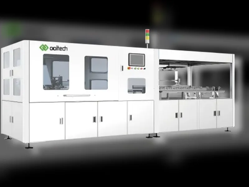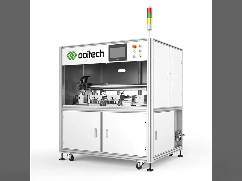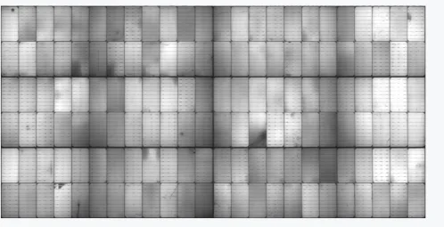
Finger Interruptions in Solar Cells — EL Testing
Table of Contents
Quick answer: Electroluminescence testing and IV testing answer different questions on a solar module line. IV testing measures how much power a module produces; EL testing shows where inside it the current is not flowing. A finger interruption — a break in the thin metallisation line that collects current from a cell — is invisible to a power measurement if the loss is small, but it appears clearly in an EL image as a dark line, because the camera images the module's own emission at wavelengths around 1200 nm. That difference matters for corrective action: an IV result tells you a module underperforms, while an EL image tells you which process step caused it, whether that is screen printing, firing, or handling damage after metallisation. Running both gates inline is what makes a defect traceable to a station rather than to a batch.
PV Module Manufacturing · by Jerry, Ooitech
Product Introduction
EL Testing and IV Testing in Solar Module Manufacturing
In a solar panel production line, two inspection steps are especially important: EL testing and IV testing. IV testing is normally used as the final performance inspection. It confirms whether the finished PV module meets the required output power before shipment.
However, IV testing measures the electrical performance of the whole module. It cannot accurately locate defects in a single solar cell, such as hidden micro-cracks, broken fingers, poor soldering, or local contamination. This is where EL imaging becomes very useful. EL testing makes invisible internal problems visible, helping production teams identify defects before the module reaches the customer.
EL testing is mainly used for qualitative location analysis of cells inside a PV module. It can help detect micro-cracks, broken cells, interrupted grid lines, weak soldering, desoldering, dirt contamination, poor sintering, and uneven cell efficiency.
Technical Parameters
Basic Technical Logic of EL Imaging
The operating principle of EL testing is closely related to the working principle of a solar cell. A crystalline silicon solar cell is mainly made from P-type and N-type semiconductor materials. When P-type and N-type regions form a PN junction, a built-in electric field is generated at the contact interface.
Under sunlight, photon energy excites electron-hole pairs. Electrons are driven toward the N region, while holes are driven toward the P region. This charge separation creates current, which is the basic power generation principle of a solar cell.
But what happens if we reverse this process?
During EL testing, the probes of the tester contact the positive and negative busbars of the PV module. Then, an external voltage is applied to the module. This voltage is conducted through the busbars, transferred to the ribbons, then delivered to the silver electrodes on the cell surface. From there, the current enters the P-type and N-type semiconductor regions inside the cell.
As electrons and holes move directionally, they form a current loop. When these carriers enter the PN junction area, also called the depletion region, radiative recombination occurs. During recombination, electrons move from a higher energy level to a lower energy level and release excess energy. This energy is emitted in the form of photons, producing near-infrared light with a wavelength of about 1100-1200 nm.
A professional EL camera captures this near-infrared light and generates the EL image.
| Item | Description |
|---|---|
| Test Method | Electroluminescence imaging under forward bias |
| Main Purpose | Visual inspection of internal solar cell defects |
| Applied Object | Solar cells and finished PV modules |
| Key Physical Process | Carrier injection and radiative recombination |
| Light Emission Range | Near-infrared light, about 1100-1200 nm |
| Detectable Defects | Micro-cracks, broken cells, broken fingers, weak soldering, desoldering, contamination, uneven efficiency |
| Main Difference from IV Test | EL locates defects visually; IV measures overall electrical output |
It should be noted that both electrons and holes are carriers. Their directional movement can be simply understood as current flow.
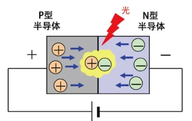
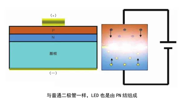
A small note: the working principle of EL testing is similar to the working principle of an LED lamp. Therefore, when the term radiative recombination appears, it does not mean that solar modules generate harmful radiation.
Technical Advantages
Why Defects Become Visible in EL Images
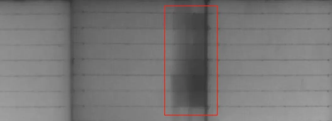
In EL imaging, any defect that affects current transmission, or more precisely carrier transmission, may become visible. If electrons or holes cannot pass through a certain area smoothly, radiative recombination will weaken or stop in that area. As a result, fewer photons are emitted, and the area appears darker in the EL image.
Micro-cracks: A hidden crack refers to a tiny crack inside the solar cell that is difficult to see with the naked eye. Although it may look invisible from the outside, for carriers such as electrons and holes, the crack is like a barrier. Carrier transmission is blocked at that location, so radiative recombination does not occur normally. Without photon emission, the crack appears as a black line in the EL image.
Weak soldering: Weak soldering usually appears as local dark spots or dark lines in EL images. These defects are often distributed along the grid line direction and may appear as irregular, discontinuous black lines or dotted dark areas. The main reason is that the ribbon and grid line do not form an effective metallic connection. This greatly increases contact resistance. Current transmission is blocked in the weak soldering area, so carriers cannot efficiently pass through that position into the cell. The luminous intensity is reduced, forming a clear dark area compared with adjacent normal cells.
Broken fingers: Broken fingers occur when the fine front grid lines of the solar cell are interrupted or separated from the cell surface. The current injected from the busbar cannot reach the disconnected fine-grid area, or the current on the finger cannot enter the PN junction inside the cell. In this area, the PN junction current density becomes very low or even zero, resulting in weak emission or no emission. This forms a typical broken-finger abnormality in EL images.
Product Application
Role of EL Testing in Solar Module Quality Control
EL testing is widely used in solar module manufacturing because it gives production engineers a direct way to inspect cell-level defects. It is especially important after key mechanical or thermal processes, where cells may be stressed or damaged.
Common application points include:
Incoming cell inspection: To check whether solar cells already have cracks, color differences, broken grid lines, or uneven efficiency before module assembly.
After stringing: To identify cracks, weak soldering, ribbon offset, or finger interruption caused during tabber stringer operation.
After layup and bussing: To confirm whether strings are correctly connected and whether welding defects appear before lamination.
After lamination: To inspect whether thermal pressure has caused new cracks or expanded existing defects.
Final module inspection: To support quality grading together with IV testing and visual inspection.
In practical production, EL testing and IV testing are not substitutes for each other. IV testing tells the manufacturer whether the module power is qualified. EL testing tells the manufacturer why a module may be abnormal and where the defect is located. When both are used together, the factory can build a more complete quality control system.
Contact Purchase
Practical Takeaway for PV Module Manufacturers
EL testing can reveal hidden micro-cracks because the crack blocks carrier movement inside the solar cell. Once carrier transmission is interrupted, radiative recombination becomes weak or disappears in that region, and the EL image shows a dark line or dark area. This is why EL testing is one of the most effective inspection methods for identifying internal cell defects that cannot be seen by the naked eye.
For PV module factories, the value of EL testing is not only finding bad modules. More importantly, it helps trace defects back to process steps such as cell handling, stringing, soldering, layup, lamination, and final assembly. This makes EL inspection a key tool for improving yield, reducing customer complaints, and stabilizing module quality.
Ooitech's View
As an equipment supplier focused on solar panel production lines, Ooitech sees EL testing as more than a simple inspection station. The real value is process feedback: if micro-cracks frequently appear after stringing or lamination, the factory should not only reject the defective modules, but also review handling stress, soldering temperature, ribbon tension, and lamination parameters. For modern MBB, TOPCon, and large-size cell modules, a well-positioned EL inspection strategy can greatly reduce hidden quality risks before shipment.