Why BC Cells Are Hard to Make: AIKO's Self-Masked Two-Step Process Explained
Table of Contents
The hard part of a back-contact (BC) solar cell is not the front. It is the back, where two oppositely doped passivating contacts have to alternate across the same wafer, and where the process conditions that suit one of them tend to spoil the other. AIKO’s answer — what the company calls its self-masked two-step process, and what Chinese industry coverage brands SeparaTech — is to stop trying to form both contacts in one pass, and to let the diffusion films that form anyway do the masking. It is a manufacturing argument, not a materials one, and that is exactly why it is worth reading from the module side.
The Difficulty Is on the Back
BC moves both polarities to the rear, so nothing shades the front and there is no front metal–silicon contact to recombine at. That is the whole point of the architecture, and it is also the source of the problem: the rear now has to carry an interdigitated pattern of P-type contact, isolation, N-type contact, repeating across the wafer.
On a passivating-contact BC cell, each of those regions may contain an ultra-thin tunnel oxide, a doped polysilicon layer, and a local metal contact. The two polarities do not want the same things:
- Oxide thickness. The window that gives good tunnelling and good passivation is not identical for the boron-doped and phosphorus-doped side.
- Polysilicon thickness and doping. N+ and P+ poly-Si have different optimum dopant profiles and different sensitivity to the thermal budget.
- Diffusion depth and annealing. The anneal that crystallises and activates one region can disturb the interface state of the other.
- Interface defects and metal contact. Contact resistivity and recombination behave differently on the two sides.
That produces the central contradiction of BC manufacturing. The device wants each region at its own optimum. A conventional flow wants one set of process conditions to serve both, to keep the number of mask, pattern, etch, clean and strip steps down.
One Step versus Two
AIKO frames the conventional approach as a one-step process: form the tunnel oxide and the polysilicon layer for both polarities together, then pattern. The argument against it is straightforward — one recipe that is right for N+ poly-Si is not necessarily right for P+ poly-Si, and adjusting the oxide thickness, the doping or the thermal budget to rescue the P side can cost you the N side. What you end up with is a compromise between the two.
| Approach | How the P and N regions are handled | Consequence |
|---|---|---|
| Conventional one-step | Oxide formation, deposition and thermal steps largely shared between the two polarities | Fewer steps, but a process compromise across the P/N boundary |
| AIKO two-step (SeparaTech) | P-type passivating contact formed first; regions then defined and the N-type passivating contact formed afterwards | More process organisation, but each region gets its own optimisation window |
AIKO’s own description of the result is that decoupling the two lets each side be optimised independently, which raises passivation quality and therefore efficiency; the company states that the process has laid the foundation for ABC cells above 27% in mass production. That is a company claim, made in AIKO’s own published material rather than by an independent test house, and it should be read as such.
The Process in Sequence
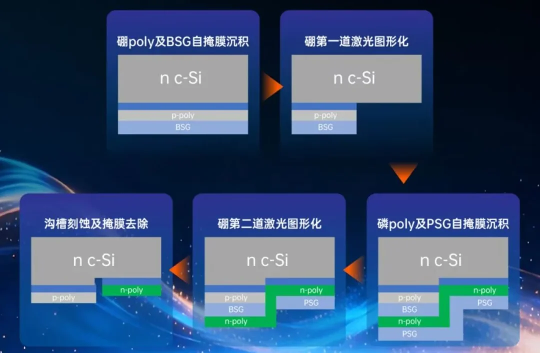
Based on the process description circulating in Chinese industry coverage, which cites AIKO patent text and public materials, the flow runs roughly like this:
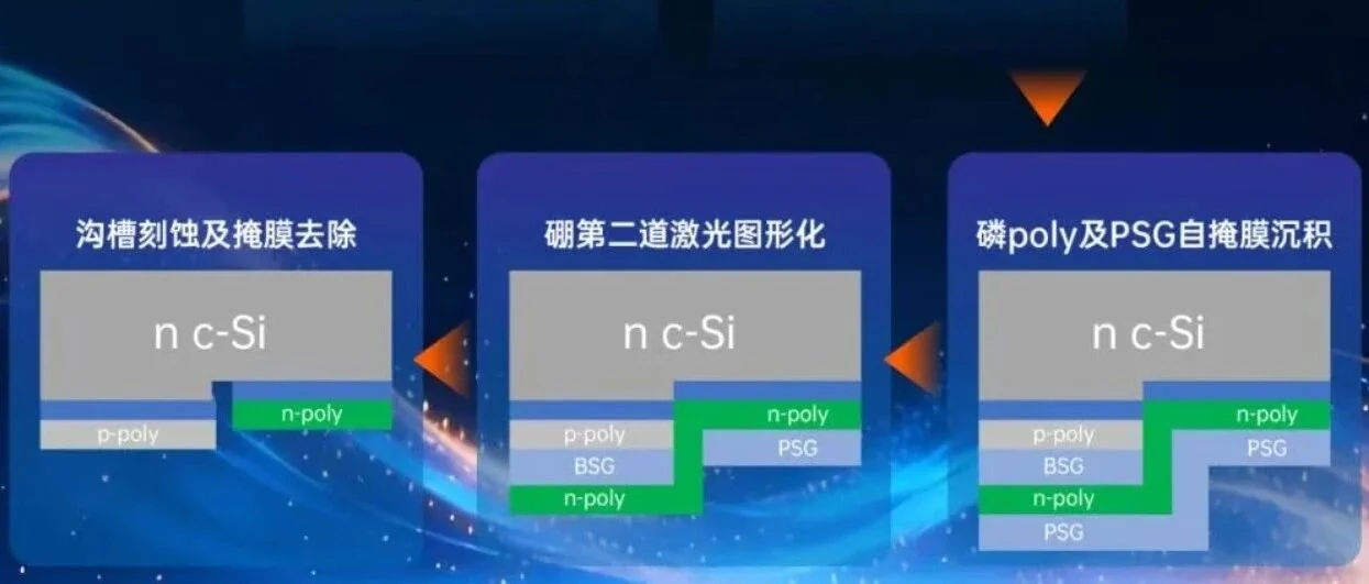
- Form the P-type passivating contact first — tunnel oxide, boron-doped polysilicon, the P+ region — with boron silicate glass (BSG) forming on the surface as a by-product of the boron diffusion.
- Use a first laser patterning step to open the positions that will become the N region and the isolation region.
- Selectively etch or alkaline-polish the exposed P-type structure away in those openings.
- Form a new tunnel oxide and N-type polysilicon, phosphorus-doped, with phosphorus silicate glass (PSG) forming on the surface.
- Use a second laser step and local removal to define the final P, N and isolation regions.
The important framing is that this is not a new material. It is the same set of layers, re-ordered in time and space and then re-integrated by patterning. The claim is about sequence and control, not chemistry.
The Diffusion Films Are the Mask
This is the part that carries most of the cost argument. BSG and PSG are not exotic layers — they form naturally during boron and phosphorus diffusion. In a conventional flow they are treated as residue to be removed. The two-step route keeps them and uses them as self-aligned masks for the subsequent patterning and selective etch.
AIKO’s stated benefits are that this removes the need for external masking and cleaning, reduces contamination risk and material consumption, and keeps the overall process complexity comparable to a one-step flow. The company also describes reconstructing the high-temperature thermal environment through thermal field simulation to balance laminar flow against passivation kinetics, with temperature control held within plus or minus 0.5 °C inside the reaction chamber, plus a stress-balancing system to keep the films low-stress and uniform.
The honest caveat is that using a diffusion film as a mask is not a new idea — early IBC patent literature contains similar thinking. What is claimed here is the specific combination of films, the process order, the laser parameters, and the ability to hold all of it across a production line.
Laser Patterning: Micron Control, and Its Own Constraints
Once the P and N regions are formed in separate passes, something has to define where each one sits. That is the laser patterning step, and its tolerance is set by geometry rather than by optics:
- Spacing too wide — you lose effective generating area.
- Spacing too narrow — any misalignment or lateral diffusion turns into a short-circuit risk, and the isolation region has less room to do its job.
Region size, edge quality and isolation width all feed into series resistance, recombination, leakage and yield at the same time. Lithography could hold the tolerance, but its cost, takt and cleanroom requirements do not fit a 10 GW or 20 GW photovoltaic line. Laser brings high-speed scanning, digital control and no resist, and brings its own problems: thermal damage, edge ablation, film residue and uniformity over a large area.
AIKO’s 2026 half-year report reportedly lists ultrafast laser patterning alongside the two-step process as a core ABC process, which is a fair indication of where the engineering effort sits.
What the Two-Step Process Does Not Fix
Even with the regions formed in separate passes, they are still on the same wafer. The second high-temperature step can affect what the first one built:
- Crystallisation state and dopant distribution of the first polysilicon layer
- The tunnel oxide already formed
- Interface hydrogen passivation
- Cross-contamination between the boron and phosphorus systems
- Recombination at the isolation region, pattern alignment, and lateral diffusion under the second thermal budget
So the accurate description is not that the two regions become independent. It is that the process order is redesigned to decouple them as far as possible, widening each one’s independent optimisation window. That distinction matters when you read a claim about “independently optimised” contacts.
The Number That Actually Decides
The framing that makes this article useful beyond one company is the economics. BC industrialisation is not decided by cell efficiency alone. The figure that matters is:
efficiency gain × yield ÷ manufacturing cost
Every extra patterning, etch, clean or alignment step moves all three terms. It adds capital and operating cost, it consumes takt, and it creates another opportunity for breakage. Which is why the observation from the process side is worth repeating: at gigawatt scale, removing one mask or one clean step can be worth more than another 0.05% of laboratory efficiency. The requirement is not a record cell — it is hundreds of thousands of wafers a day with the P/N pattern still aligned.
What Reaches the Module Line
This is where it lands for us, and it is a point that gets lost when BC is discussed only as a cell technology.
BC is a device architecture, not a single process route. HPBC, ABC, N-type passivating-contact BC and GPC all look the same from the front — no front electrode, carriers collected at the rear — but underneath they can differ in carrier-selective contact, how the P and N regions are formed, how they are patterned, the isolation structure, the metallisation, and whether the flow can reuse an existing TOPCon line. We covered the naming side of that in Is BC just one technology? and the structural side in the BC technology roadmap.
For a module line, the consequence is concrete:
- Cells that look identical at the front are not identical to handle. Rear contact layout and pitch differ between BC variants, and that sets the soldering process, the placement tolerance and the inspection recipe.
- The process change is happening upstream of the module line but the mechanical consequences land on it. A tighter rear pattern means a tighter placement window; a thinner or more highly stressed cell means more handling loss between the cutter and the laminator. BC bowing and warpage is already a known issue on the module side, and we have written about why BC cells bow more and why BC strings warp.
- The back-end metallisation route changes the interconnection entirely. The cost problem moves to the rear electrode, which is why low-silver and copper-based metallisation and zero-busbar designs are being pushed at the same time as the front-end process. The silver-free debate and the need for insulating glue on the rear both arrive at the stringer, not at the furnace.
- The same economics rule applies downstream. A module line buying a BC-ready stringer is making the same calculation the cell maker makes: capability gain × yield ÷ cost. A machine that adds a process but costs yield has not helped.
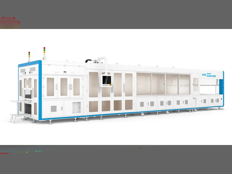
What the cell-side process innovation changes for us is not a new machine category. It is the specification of the existing stations — the SC-20P back-contact laser cutting platform, the OSLB-1300 back-contact cell stringer and the SL-1000 back-contact welder — because those are the stations that see the rear pattern first.
Timeline and the Published Numbers
| Milestone | Reference |
|---|---|
| N-type All Back Contact (ABC) invented | AIKO technology timeline, 2019 |
| ABC cell efficiency reached 26.5% | AIKO presentation to the 2023 Back Contact Workshop |
| Zhuhai first-phase 6.5 GW ABC cell line in production | Reported in Chinese industry coverage, 2022 |
| Self-masked two-step process described publicly as commercialised | AIKO published material and PV Tech industry update, July 2025 |
| ABC cells above 27% stated as the mass-production foundation | AIKO published material, July 2025 (company claim) |
| 2282 ABC-related patent applications, 820 granted, 234 granted invention patents | AIKO 2026 half-year report, as cited in Chinese industry coverage |
| G4 full-screen Ultra module stated at 26% maximum efficiency, up to about 690 W in standard format | AIKO 2026 product announcement (launch specification) |
One caution that the source coverage makes well and that is worth keeping: a product launch figure and a third-party commercial ranking are not the same measurement. As of September 2026, third-party commercial module rankings place AIKO’s listed products at 25.0% maximum efficiency, jointly first with LONGi. A launch specification of 26% and a commercial listing of 25.0% describe different stages of the same product, and it is a mistake to compare them as if they were the same number.
Frequently Asked Questions
Is the two-step process a new material or a new process?
A new process. The layers are the same families — tunnel oxide, doped polysilicon, metal contact. What changes is the order in which the P and N sides are formed and how the regions are defined afterwards.
Why can the two regions not simply be optimised in one pass?
Because several of the key parameters are shared. Oxide thickness, deposition conditions and thermal budget each set the quality of both contacts at once, and the optimum for boron-doped poly-Si is not the optimum for phosphorus-doped poly-Si. One pass means a compromise somewhere on the wafer.
What is meant by self-masked?
The boron and phosphorus diffusion steps leave BSG and PSG on the surface as a natural by-product. Rather than stripping them, the process keeps them and uses them as the mask for the following patterning and selective etch, which removes several external mask, coat, expose, strip and clean steps.
Does this solve BC cost entirely?
No. It addresses the front-end device manufacturing. The rear electrode cost is a separate problem, which is why low-silver and copper-based metallisation and zero-busbar interconnection are being developed in parallel. A very efficient cell that still needs a large amount of silver paste to connect is not yet an economically complete answer.
Does a better cell process make the module line easier?
Not automatically. It can make it harder. A tighter rear pattern raises the placement requirement, and any change in cell stress or thickness shows up as handling loss and breakage on the assembly line. The cell-side gain and the module-side cost have to be considered together.
Where does the information in this article come from?
Three places, and they carry different weight. The process description, the SeparaTech name, the patent counts and the efficiency-times-yield framing come from the Chinese industry article published by 新能供应链, which cites AIKO patent text, the 2026 half-year report and public company materials. The English process description and the claims about efficiency above 27% come from AIKO’s own published material, republished as an industry update by PV Tech — that is company-authored content and we have labelled it as a claim rather than an independent result. The ABC efficiency and timeline figures come from AIKO’s presentation to the 2023 Back Contact Workshop. Nothing in this article is based on our own measurement of a BC cell or of AIKO’s process.