BC Cell Technology Roadmap: Structure to Process
Table of Contents
TOPCon, IBC, TBC, HBC and HIBC are usually listed as a family tree of acronyms. They are better read as a sequence of problems: each route exists because the previous one left a specific loss unsolved, and each one moves the difficulty somewhere else.
PV Cell Technology · Back Contact Routes · by Jerry, Ooitech
1. TOPCon: Get the Passivation Contact Right First
TOPCon uses an ultra-thin silicon oxide layer plus a doped polysilicon layer to form a passivation contact. The SiOx film handles interface passivation; the doped polysilicon handles carrier-selective transport. Oxide thickness, polysilicon doping concentration and the annealing recipe are the three knobs, and together they lower recombination at the contact while keeping transport loss low.
The problem being solved is contact recombination. A conventional metal contact touching silicon directly produces strong interface recombination. By separating passivation from carrier selectivity, TOPCon reaches a higher open-circuit voltage. It does not, however, remove the front metal grid, so front-side shading remains.
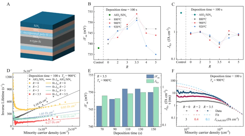
Fig. 1: A carbon-doped intrinsic polysilicon passivation contact, with the structure at left and the resulting iVoc, J0s and lifetime data across deposition conditions at right. Work published in 2025 pushed surface saturation current density below 0.5 fA/cm² and connected the structure to back-contact applications.
2. IBC: Move the Front Metal to the Back
IBC makes a blunt structural change: both the n-type and p-type contacts move to the rear. The front of the cell carries no metal grid at all, which frees the front surface for optical management and passivation design. With less front metal blocking light, the number of photons entering the wafer rises and short-circuit current has more room to grow.
The cost appears on the back. Where a conventional cell separates the two polarities across different faces, IBC has to alternate n-type and p-type contacts on one surface, keep them electrically isolated, and then metallise both. Contact width, n/p spacing, the polarity boundary, contact resistance and grid geometry all become coupled variables on a single plane.
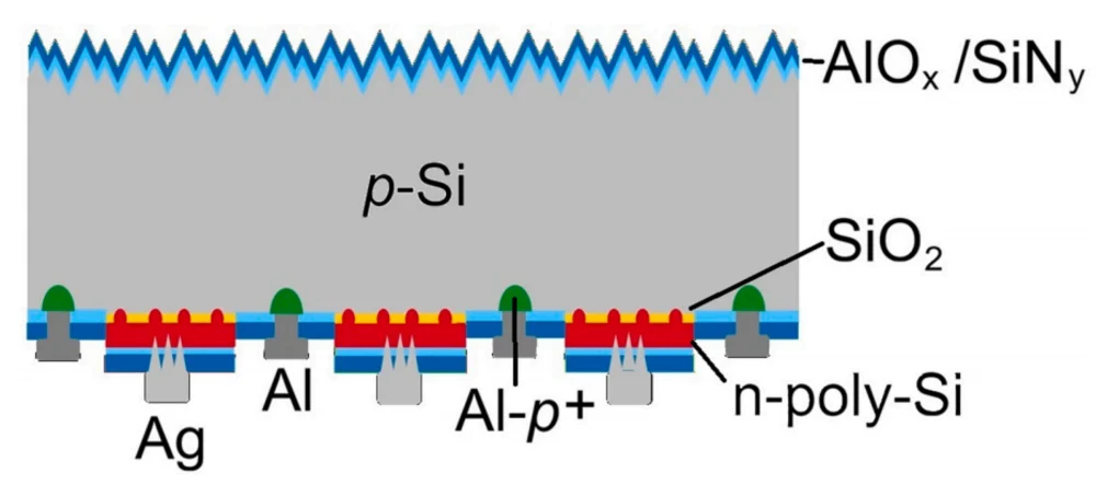
Fig. 2: A simplified POLO-IBC stack. In 2026, POLO-IBC cells fabricated on M2-size wafers with industrial equipment reached 24.5 percent certified efficiency. The loss analysis pointed at front surface passivation, recombination at the silver contact to the n-type polysilicon region, and recombination and contact resistance in the aluminium region as the main targets.
3. TBC: TOPCon Enters the Back-Contact Structure
TBC is the union of the previous two: TOPCon supplies the passivation contact, IBC supplies the back-contact architecture. The result is n-type and p-type passivation contacts formed on the rear, with the front staying free of metal.
The advantage comes from inheritance. TBC builds on material and process work that TOPCon has already industrialised. The difficulty that remains is specific: the p-type passivation contact. Its interface recombination and contact behaviour feed directly into cell voltage and fill factor, which makes it the gating item rather than an optimisation detail.
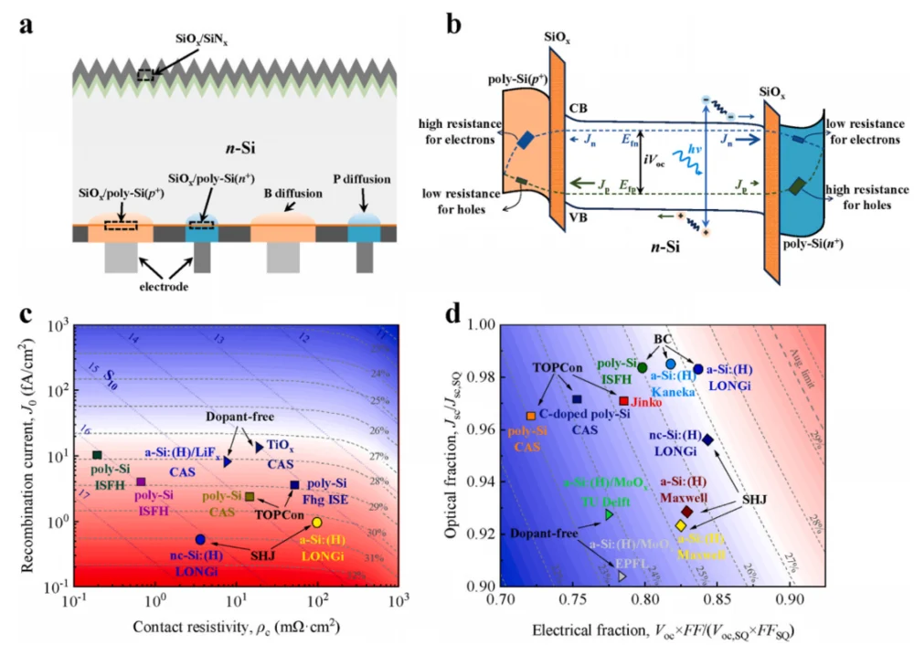
Fig. 3: TBC structure and band diagram (a, b) with efficiency-potential maps (c, d). A 2025 simulation study of device parameters concluded that TBC has efficiency potential approaching 28 percent once wafer quality, surface passivation, the p-type contact and the rear structure are jointly optimised.
The more consequential TBC research is about process, not structure. If a manufacturer can reuse the mature poly-Si/SiOx passivation stack from TOPCon and only rework rear patterning and metallisation, the distance between a BC line and an existing TOPCon line shrinks considerably. That is why TBC work has moved from the contact stack itself toward contact performance, patterning sequence and metallisation.
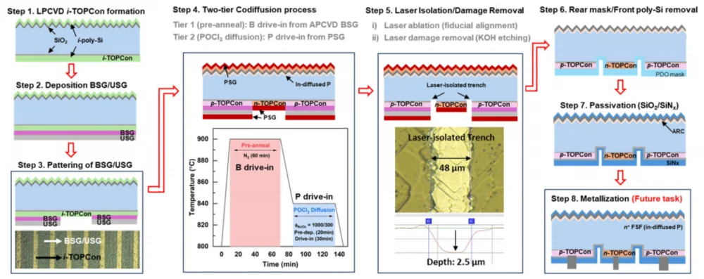
Fig. 4: A low-cost co-diffusion route to a TBC precursor, from LPCVD i-TOPCon formation through two-tier co-diffusion, laser isolation, rear mask removal and passivation. Two-tier diffusion with a single thermal budget is what keeps the step count and the thermal exposure manageable.
4. HBC: The Same Idea From the Heterojunction Side
TBC enters back contact through TOPCon. HBC enters through silicon heterojunction: SHJ supplies the passivation contact, IBC supplies the back-contact structure, and both polarities end up on the rear.
SHJ forms its contact from intrinsic and doped amorphous silicon, which delivers high interface passivation quality. Combined with the front-side gain of IBC, HBC has strong voltage and current potential. LONGi reported a 27.30 percent HBC cell in 2024, certified by ISFH in Germany.
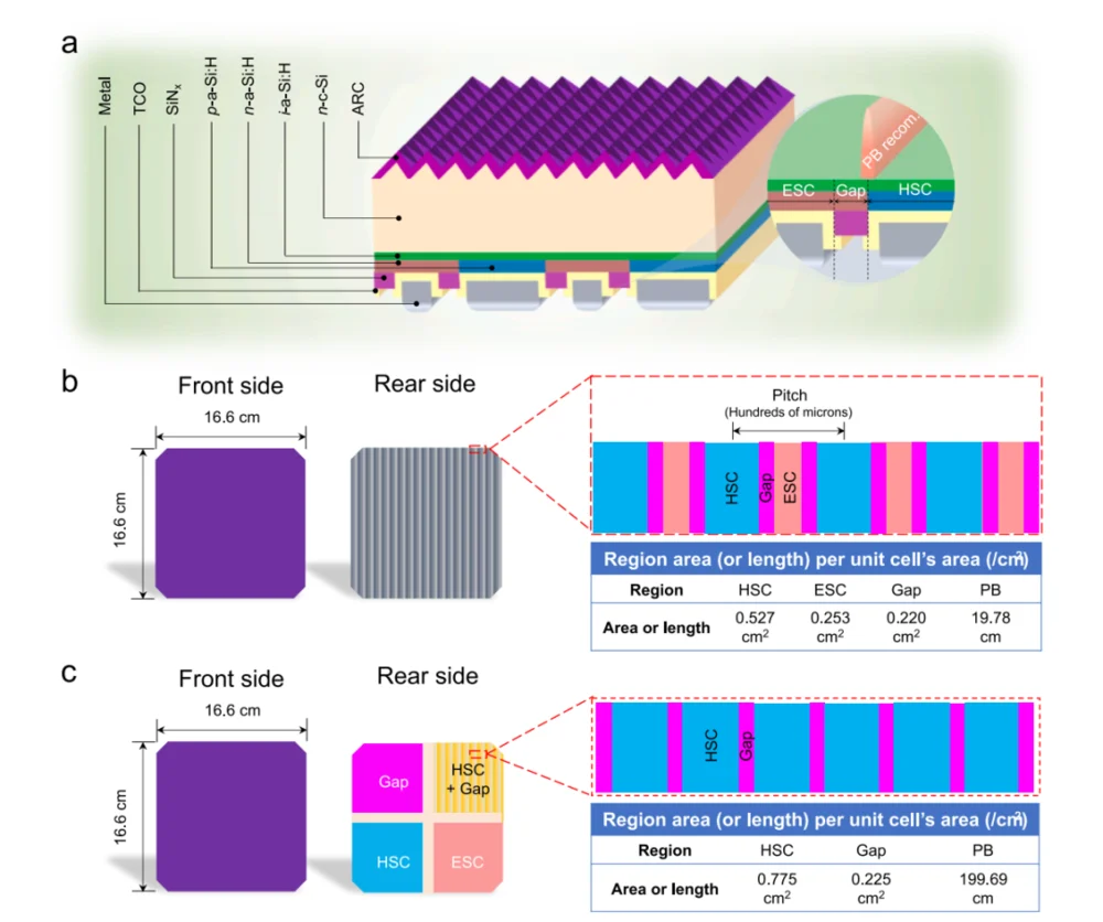
Fig. 5: An HBC stack with the polarity boundary highlighted (a), and two rear layouts with their region areas (b, c). The gap between the electron-selective and hole-selective regions is narrow, and recombination there is a loss mechanism in its own right rather than a side effect of the heterojunction.
HBC optimisation therefore cannot stop at the heterojunction. Because n-type and p-type contacts sit next to each other on the rear, the polarity boundary between them becomes a distinct recombination source that drags on fill factor. Research in 2025 analysed this boundary specifically, and it is one of the clearest illustrations of the general BC problem: the more functions you pack onto one surface, the more the interfaces between them matter.
5. HIBC: Different Passivation Contacts on One Cell
TBC and HBC each commit to a single contact system. HIBC asks a different question: if different passivation contacts have different strengths, can they be assigned to different regions of the same rear surface according to what each region needs?
The answer published in Nature in 2025 was yes. HIBC combines a high-temperature polysilicon tunnel contact with a low-temperature heterojunction contact on the same rear surface, and uses laser processing to locally enhance transport in the p-type contact. The result was 27.81 percent conversion efficiency at 87.55 percent fill factor.
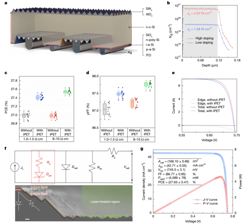
Fig. 6: HIBC device results, including the layer stack with the laser-treated region (a), doping profile (b), efficiency and fill-factor distributions with and without the laser treatment (c, d), the equivalent circuit and cross-section (f), and the J-V curve (g). Note the vocabulary has changed from "which structure wins" to "which region needs what".
The conceptual move matters more than the number. A BC rear contains several functional regions, and those regions do not have identical requirements for passivation, carrier selectivity, contact resistance and metallisation. HIBC configures contacts per region instead of applying one contact technology across the whole cell. That is a different design philosophy, and it is the point at which the roadmap stops being a ladder.
6. From Structure Innovation to Process Collaboration
Put the five routes in one line and the pattern is clear: each step solves a recombination or optical problem and hands the next step a manufacturing problem.
| Route | Core technology | Problem solved | Current focus |
|---|---|---|---|
| TOPCon | SiOx / poly-Si passivation contact | Contact recombination | Passivation quality, contact resistance |
| IBC | n and p contacts both on the rear | Front metal shading | Rear structure, polarity boundary, metallisation |
| TBC | TOPCon + IBC | Contact recombination without front shading | p-type contact, process compatibility with TOPCon lines |
| HBC | SHJ + IBC | Highest passivation quality with no front metal | Polarity boundary recombination, rear patterning |
| HIBC | Poly-Si tunnel contact + heterojunction contact, region by region | Optimising each rear region by function | Laser-localised contact enhancement, integration |
The higher the efficiency, the more complex the rear surface, and the tighter the process window. n-type contacts, p-type contacts, polarity boundaries, metal grids and local openings all have to stay within tolerance simultaneously. A dimensional drift or a process fluctuation in any one of them shows up as contact resistance, recombination loss or degraded current collection. This is the substance of the phrase "from structure innovation to process collaboration": efficiency leadership now depends on holding several coupled processes stable at once.
7. Metallisation: Efficiency and Silver Have to Be Optimised Together
BC metallisation is not a scaled-up version of front-side printing. Both polarities are on the rear, so the grid has to collect current within a confined area while maintaining electrical isolation between adjacent opposite-polarity regions. Finger width, finger pitch, busbar, contact pad and contact area each affect performance, and they interact.
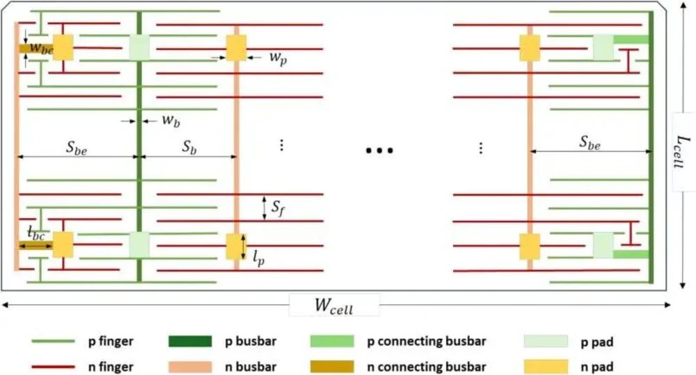
Fig. 7: Rear metallisation parameters for a TBC cell. Finger geometry, busbar arrangement, connecting busbars and pad dimensions are not independent choices; each one trades series resistance against printing precision and silver consumption.
A 2026 study of TBC grid design analysed these parameters systematically and put cell efficiency and silver paste consumption into a single optimisation framework, covering finger width, finger pitch, busbar, contact pad and zero-busbar layouts. The practical conclusion is that BC metallisation has to be optimised on four axes at once: contact resistance, series resistance, printing accuracy and silver consumption.
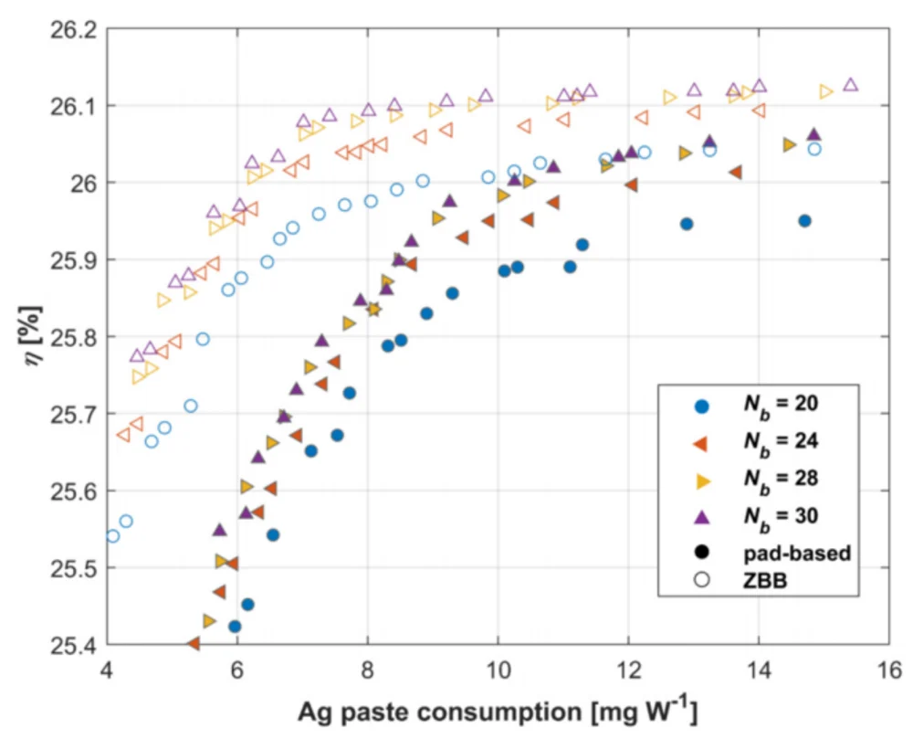
Fig. 8: Efficiency against silver paste consumption for different busbar counts and for pad-based versus zero-busbar (ZBB) layouts. The curves flatten, which means the last increments of efficiency become progressively more expensive in silver, and the choice of layout shifts the whole curve rather than a single point on it.
This is where research starts to look like procurement. Silver is a recurring cost that scales with production volume, and a grid design that buys two tenths of a percent of efficiency with a large increase in paste consumption is a different commercial proposition from one that reaches the same efficiency with a leaner print.
8. Low-Cost IBC: Removing Lithography From the Flow
IBC's manufacturing complexity has always been a central industrialisation question. Forming interleaved n-type and p-type regions on the rear traditionally relies on photolithography and laser steps, and each additional step adds equipment, cycle time and cost.
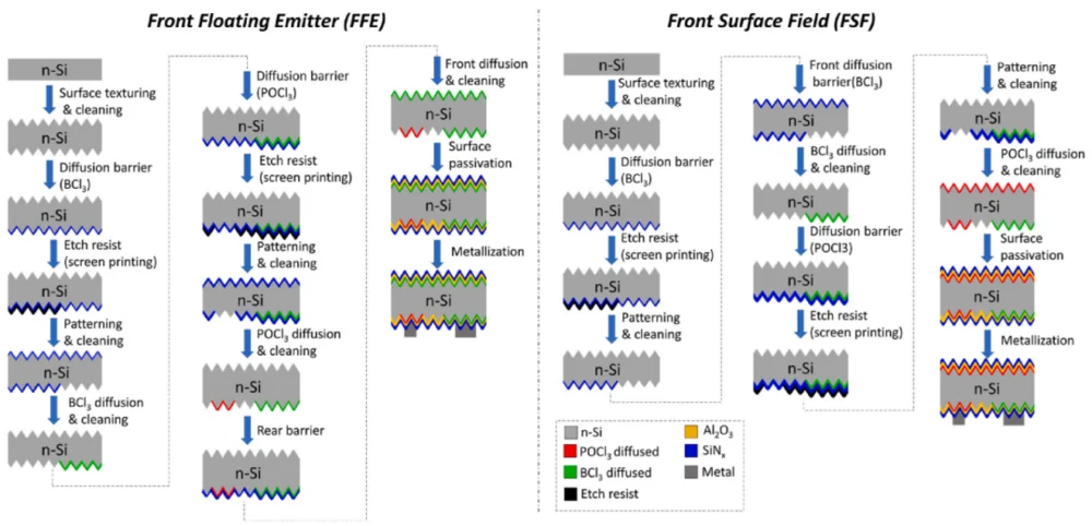
Fig. 9: Two lithography-free IBC flows built on screen-printed diffusion barriers, using either a front floating emitter or a front surface field. Both rely on equipment already standard in cell lines rather than on new process platforms.
A 2026 study demonstrated a fully screen-printed, lithography-free and laser-free IBC route, using a patterned SiNx diffusion barrier to achieve selective boron and phosphorus diffusion and completing the cell on mature industrial equipment, reaching 19 percent-level IBC cells. The headline number is deliberately unspectacular. What the work answers is whether IBC can be built with fewer process steps on equipment that already exists, and that question matters more to equipment investment and production cost than another laboratory record.
Read alongside the metallisation work, the direction is consistent: the frontier is no longer "can this structure reach 28 percent", but "can this structure be produced repeatably, with fewer steps, on tools that can be serviced and supplied at industrial scale".
9. What This Means for Equipment Selection
If the bottleneck has moved from structure to process, then the equipment decisions that matter have moved with it. Four of them are worth weighing before a BC line is specified.
| Decision | Why it follows from the roadmap |
|---|---|
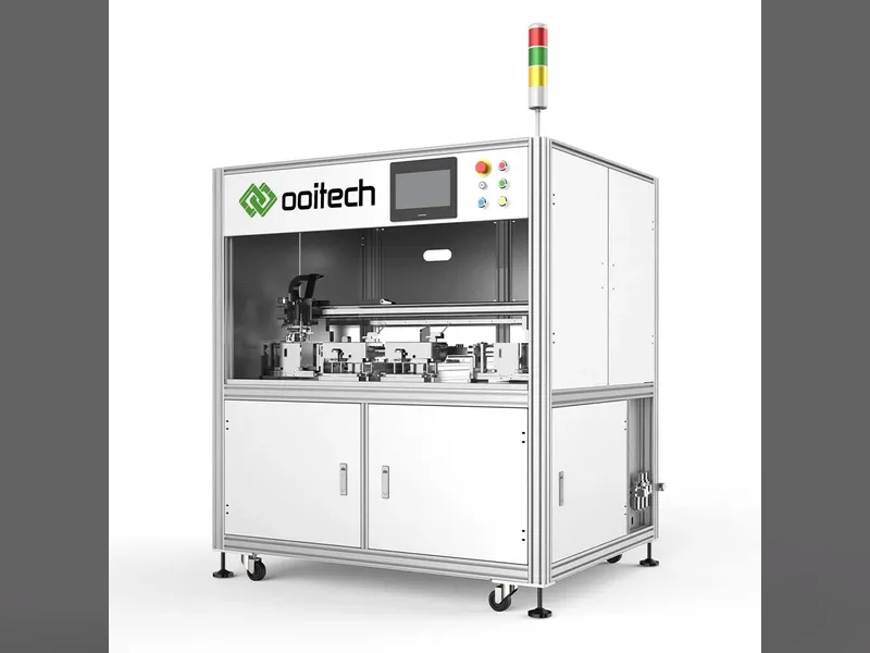
| Cutting and edge quality | Every BC route depends on a rear surface where several functions sit close together. Laser cutting and scribing quality set how much of that surface is degraded before any contact is formed. Our SC-20P BC cell laser cutting machine is specified around this step. |
| Soldering on a single face | In IBC, TBC and HBC all interconnects land on one surface next to opposite-polarity structures, so placement tolerance and thermal control matter more than on a conventional cell. |
| Inspection depth | A polarity-boundary or contact defect has no reliable optical signature. EL and IV testing per module barcode is what converts a latent fault into a detected one, as covered in EL testing: inline vs offline setup. |
| Process step budget | The low-cost IBC work exists because step count drives cost. Equipment that merges stations or removes a lithography step changes the economics more than a marginal efficiency gain. |
This is also why the routes are not competing for the same factory. TBC inherits TOPCon process maturity and suits manufacturers already running poly-Si lines. HBC suits those with heterojunction capability. HIBC is a region-by-region design philosophy rather than a line configuration you can buy today. And low-complexity IBC targets manufacturers who want back contact without building a lithography-based flow. The choice is a function of what you already run.
FAQ
What is the difference between IBC, TBC and HBC?
All three are back-contact structures, meaning both polarities are on the rear and the front carries no metal grid. They differ in how the contact is formed. IBC is the base architecture. TBC forms its rear contacts using TOPCon's SiOx/poly-Si passivation contact. HBC forms them using silicon heterojunction contacts made from intrinsic and doped amorphous silicon.
What is HIBC?
Hybrid interdigitated back contact. Instead of applying one contact technology across the whole rear, HIBC assigns different contact types to different rear regions according to what each region needs, combining a high-temperature polysilicon tunnel contact with a low-temperature heterojunction contact and using laser processing to locally enhance the p-type contact. The 2025 Nature result was 27.81 percent efficiency at 87.55 percent fill factor.
Why is the polarity boundary a problem?
Because the two polarities sit next to each other on the same surface. Where an electron-selective region meets a hole-selective region, recombination at that boundary acts as an additional loss path and reduces fill factor. It is a direct consequence of packing both contacts onto one face, and it is why HBC optimisation cannot stop at the heterojunction itself.
How much silver do BC cells use?
Enough that grid design is treated as an efficiency-versus-consumption problem rather than a purely electrical one. Recent TBC grid studies optimise finger width, finger pitch, busbar and pad dimensions together with silver paste consumption, and zero-busbar layouts are evaluated specifically because they shift that trade-off rather than merely moving along it.
Can IBC be manufactured without lithography?
Yes, and it is an active research direction. A 2026 study demonstrated a fully screen-printed, lithography-free and laser-free IBC route using a patterned SiNx diffusion barrier for selective boron and phosphorus diffusion, built on mature industrial equipment and reaching 19 percent-level efficiency. The point of the work is process simplification rather than a record efficiency.
Which route should a new factory plan for?
Start from the process base you already have rather than from the highest published efficiency. TBC is the shortest step for a manufacturer running TOPCon poly-Si lines, because it reuses that passivation stack. HBC requires heterojunction capability. Low-complexity IBC suits manufacturers who want back contact without a lithography-based flow. The published efficiency ranking and the practical entry cost are different orderings.
Final Thoughts
The five routes are best understood as one continuous problem-solving sequence rather than five competing products. TOPCon solved contact recombination and left front shading in place. IBC removed the front metal and moved the difficulty to the rear. TBC and HBC each supply a different contact system for that rear. HIBC stops treating the rear as one surface and configures it region by region. What all of them now share is that the limit is no longer the structure diagram: it is metallisation economics, edge and boundary quality, process step count and the ability to hold several coupled processes stable at once. If you are planning a BC or TOPCon format line, tell us the cell format, the contact scheme and the module format you are targeting, and we will work through the cutting, stringing and inspection configuration that fits it.