Why BC Solar Cells Are More Prone to Bowing and Warpage
Table of Contents
Quick answer: Back-contact cells are more prone to bowing and warpage than front-contact cells because both polarity contacts sit on the rear, so the rear metallisation volume and the stress it introduces are unbalanced against the front. When the cell cools after firing, the rear metal contracts against an unmetallised front face, and the result is a curvature that can be measured in fractions of a millimetre across a 182 mm or 105 mm cell. The processing temperatures involved — around 110 °C in later steps against an ambient reference near 22 °C — set how much differential contraction accumulates. Bowing matters because a warped cell does not sit flat on the stringer or in the laminate, which produces positioning errors, uneven encapsulant thickness after lamination and, in the worst case, micro-cracks at the joint.
PV Module Manufacturing · by Jerry, Ooitech
BC Solar Cell Bowing and Warpage
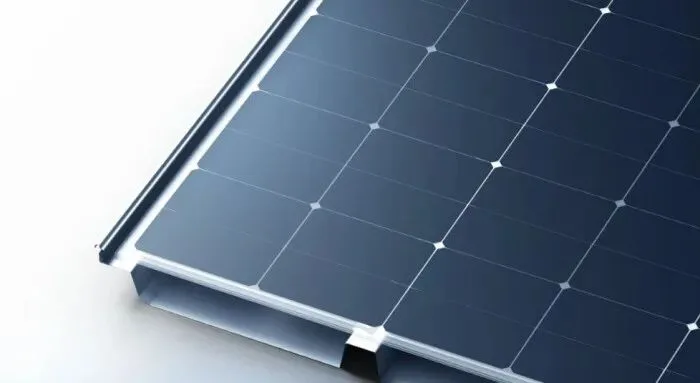
In the intense competition between photovoltaic technology routes, BC, or back-contact, solar cells stand out for their efficient and visually clean design. With no metal grid lines on the front surface, BC cells have become one of the industry's most closely watched technology directions.
Behind that clean appearance, however, lies a difficult manufacturing problem: BC cells are naturally more likely to bow and warp.
As industry specialists have pointed out, all electrodes are located on the rear side, so the cell is inherently prone to deformation. During module assembly, more materials are continuously added to the back, including insulating adhesive, solder ribbons, and solder paste. As these layers build up, the warpage problem can become increasingly serious.
So, why are BC cells more susceptible to bowing and warpage than conventional solar cells?
1. Structural Asymmetry Creates an Inherent Warpage Risk
The most distinctive feature of a BC cell is that both positive and negative electrodes are placed on the rear surface. There are no metal grid lines on the front. This design improves light absorption, but it also introduces an inherent structural weakness.
Research indicates that BC cells show significantly greater warpage than TOPCon cells with electrodes distributed across the front and rear surfaces. Under similar rear-side structures, front grid lines can partly offset deformation caused by shrinkage on the back.
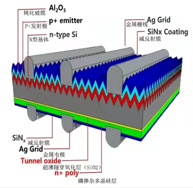
BC cells do not have these front grid lines. The resulting stress imbalance between the front and rear surfaces makes cylindrical deformation more likely during manufacturing and use.
This structural asymmetry is essentially the result of uneven stress. It is similar to the way a sunflower bends toward sunlight because of different growth rates on its shaded and illuminated sides. In a BC cell, the contraction stress generated by the multiple rear-side layers is much greater than the stress on the front, naturally causing the wafer to bend.
2. Thermal Expansion Mismatch Between Rear-Side Materials
Several functional layers must be applied to the rear of a BC cell. In addition to the conventional metal electrodes, these may include insulating materials, solder paste, and solder ribbons. Differences in the coefficients of thermal expansion among these materials are a primary driver of warpage.
The expansion difference between metal and silicon is particularly significant. Silver has a coefficient of thermal expansion approximately seven times that of silicon. During cell manufacturing, this difference can generate substantial thermal stress between the silver metallization and the silicon substrate. Warpage may become even more severe after solder paste is printed.
Insulating materials also play an important role. Insulation is required to separate the positive and negative electrodes on the rear surface, but the thermal expansion coefficient of the insulating material differs from that of the silicon wafer. If the contact area between the insulation and the cell is too large, material consumption increases and the stress caused by thermal expansion mismatch also rises. This can intensify cell warpage and lead to process risks such as cell breakage and cells sticking or overlapping during handling.
3. Single-Sided Soldering Produces Unbalanced Mechanical Stress
BC modules usually use single-sided soldering, with all solder ribbons concentrated on the rear surface. This is fundamentally different from conventional double-sided soldering.
For example, when 21 solder ribbons are attached to a 182 mm × 105 mm cell, significant warpage occurs as the temperature falls from 110°C to 22°C. This happens whether the cell thickness is 0.13 mm, 0.15 mm, or 0.18 mm.
The deformation mainly comes from uneven thermal stress generated during soldering. It is an inherent structural issue associated with the single-sided interconnection used for BC cells.
More concerning is that increasing cell thickness does not solve the problem effectively. Simulation results show that single-sided soldering can produce warpage as high as 4.9 mm. Even when cell thickness is increased to 0.18 mm, warpage decreases by only about 18%. Under the same conditions, the maximum warpage caused by double-sided soldering is only 0.07 mm.
| Soldering condition | Cell or process condition | Reported warpage behavior |
|---|---|---|
| Single-sided soldering | 182 mm × 105 mm cell with 21 ribbons | Significant warpage during cooling from 110°C to 22°C |
| Single-sided soldering | Cell thickness of 0.13 mm, 0.15 mm, or 0.18 mm | Warpage remains significant at all three thicknesses |
| Single-sided soldering | Simulation result | Warpage can reach 4.9 mm |
| Single-sided soldering | Thickness increased to 0.18 mm | Warpage is reduced by only about 18% |
| Double-sided soldering | Same comparison conditions | Maximum warpage is approximately 0.07 mm |
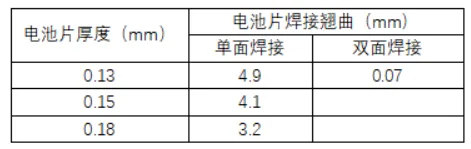
This means that achieving the warpage level of double-sided soldering through wafer thickening alone would require a thickness far beyond 0.18 mm. That would substantially increase silicon consumption and material costs.
The problem can also continue into lamination. Asymmetric warpage caused by single-sided soldering may compress the encapsulant around the cell edges and central area. The encapsulant can become thinner or even be punctured, creating local stress concentration points that threaten structural integrity and long-term module reliability.
4. Thinner and Larger Cells Amplify the Problem
The photovoltaic industry continues to pursue thinner wafers to reduce silicon costs and larger cell formats to increase module power. Both trends can make BC cell warpage more severe. Research shows that reducing cell thickness and increasing cell size both significantly increase deformation.
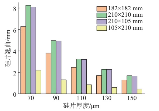
For a 210 mm × 210 mm cell, reducing thickness from 150 μm to 70 μm increases the reported warpage from 1.69 mm to 8.25 mm, nearly a fivefold rise.
| Cell size | Cell thickness | Reported warpage |
|---|---|---|
| 210 mm × 210 mm | 150 μm | 1.69 mm |
| 210 mm × 210 mm | 70 μm | 8.25 mm |
These figures clearly show the challenge created by wafer thinning. For an industry seeking both higher efficiency and lower costs, controlling warpage while reducing silicon thickness has become a technical barrier that must be addressed.
6. Industry Mitigation Strategies and Outlook
The industry is already exploring several ways to manage BC cell warpage. Common approaches include:
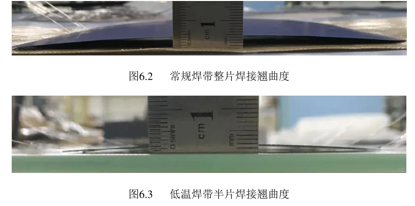
Half-cell module designs: Smaller cell dimensions can reduce the absolute bowing height.
Optimized grid-line materials and widths: Adjusting metallization structures can help manage rear-side stress.
Low-temperature soldering: Lower process temperatures can reduce thermal stress during interconnection.
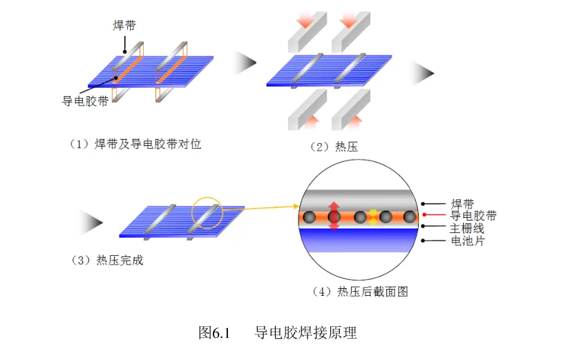
Conductive adhesive hot pressing: This provides an alternative to conventional high-temperature soldering processes.
Curved pressure-block correction mechanisms: Special correction structures can be integrated into tabber and stringer equipment to control cell shape during processing.
Low-Temperature Solder Ribbon Interconnection
References
Dong Peng, Research on High-Efficiency N-Type Back-Contact Solar Cell Processes
MeCan Solar, Warpage Behavior and Grid-Line Structure Optimization of Large-Format Thin BC Cells
Solar and Energy Storage Review, The Attractive Appearance of Single-Sided Soldering Cannot Hide Warpage and Its Related Risks
Ooitech's View
Warpage control has to be treated as a complete module-process issue, not just a cell-thickness problem. Soldering temperature, ribbon layout, pressure control, handling, and lamination must be tuned together, especially when thin and large-format BC cells are used. A small deformation left uncontrolled at the interconnection stage can become a yield or reliability problem later in the production line.