Editorial responsibility for this article rests with Wuhan Ooi Photoelectric Technology Co., Ltd. Written and reviewed by the Ooitech editorial team. See our editorial policy for how we write, where AI tools are used, and how to request a correction.
PV Ribbon Soldering: The Joint, the Window, the 0BB Shift
Table of Contents
Quick answer: A ribbon joint is finished before anyone sees it. In one to two seconds the coating melts, wets the silver grid, grows a micron-scale intermetallic layer and freezes. The peak temperature decides whether it wets; the time at temperature decides how brittle the interface becomes; the cooling that follows decides how much stress the cell is left carrying. The soldering window is therefore not set by the melting point of the solder. It is set by strain.
You can watch a stringer for a full shift and see almost none of the joint. There is a flash under the lamp box, a cooling stretch, and a string that either passes electroluminescence or does not.
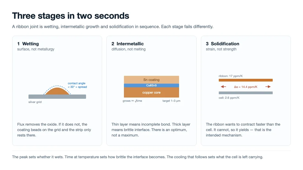
Everything that decided the outcome happened inside a window too short to observe and too fast to correct by eye. Three stages run in sequence in that flash — wetting, intermetallic growth, solidification — and each one fails differently. Reading those differences is what lets a line debug in an afternoon instead of replacing ribbon for a month.
Wetting decides whether a joint exists at all
Wetting is a surface event, not a metallurgical one. Before tin can bond to silver it has to displace the oxide on both surfaces, and that is the flux's only real job in the process. If the oxide survives, the coating beads on the grid instead of spreading across it, and a strip that looks soldered is really a strip resting on a surface.
Contact angle is the honest measure: below roughly 30 degrees the alloy is spreading, above 60 it is sitting. Nobody measures contact angle on a stringer, so the process substitutes proxies instead — pull strength, cross-section area, edge EL.
| Variable | What it sets | What it drifts with | First symptom |
|---|---|---|---|
| Temperature | Whether the coating clears its liquidus with margin, and how fast the flux activates | Emitter ageing, plate contact, set point | Unwetted strip at the cell edge |
| Time | How long flux and alloy can react before freezing | Line speed, pulse length | Joints that look complete with low pull strength |
| Pressure | Whether ribbon and grid are in actual contact | Pin wear, height drift, cell thickness scatter | Contact marks on one side only |
| Flux | Oxide removal and surface tension | Flux age, drying, applied weight | Random unwetted spots that move between runs |
The four do not substitute for each other, and that is where most corrective action goes wrong. Raising the peak to compensate for weak flux grows the intermetallic layer without fixing the wetting. Raising pressure to compensate for a cold profile embeds the ribbon and starts microcracks at the edge. The variables look interchangeable on the HMI and are not.
Flux activation is the part people get wrong most often. A flux has an activation window: it does its work over a temperature band, not at an instant. If the coating reaches its liquidus while the flux is still inactive, the wetting window is simply spent. That is one reason a profile that looks right on an emitter curve can still produce unwetted joints — the energy is there, but it arrives in the wrong order.
The intermetallic layer has an optimum, not a maximum
Where tin meets copper, Cu6Sn5 grows. At the silver grid, Ag3Sn forms. Where a nickel barrier is used, the layer is Ni3Sn4. None of this is contamination. Without an intermetallic layer there is no bond — the solder simply sits on the surface and the pull test reads whatever friction gives it.
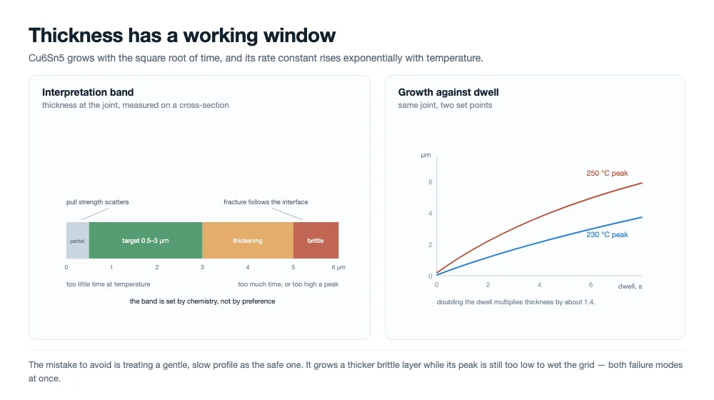
The problem is thickness, because the layer is hard, brittle, and does not stop growing when the machine stops. Growth is diffusion-controlled: thickness rises with the square root of time, and the rate constant follows an Arrhenius relationship. A doubled dwell does not double the layer, it multiplies it by about 1.4. Ten degrees of extra peak does more than that, because the rate constant moves exponentially.
Soldering practice converges on a working range of roughly 1 to 3 micrometres. Below about half a micrometre the bond is incomplete and pull strength scatters. Above roughly 5 micrometres the interface behaves like a brittle ceramic, and a fracture that starts there propagates across the whole strip rather than stopping in the solder.
The cross-section tells you which side of the optimum you are on. If the fracture runs through the solder, the interface is fine and the bulk alloy or the pull geometry is the problem. If it runs along the interface between alloy and grid, the layer is too thin or the surface never wetted. If it runs through the intermetallic layer itself, the layer is too thick and the peak or the dwell is the lever.
What the stringer controls, and what it inherits
The sequence inside a modern stringer is short: flux, place, preheat, weld, cool, EL. The welding step itself is one to two seconds of contact between a hot plate and a cold cell, and almost all of the metallurgy happens in that second or two.
Fraunhofer ISE published a validated thermal model of that step in 2025, built on an industrial infrared stringer and checked against thermocouples. In their baseline the plate preheats the cell to about 121 °C, then two pulses of roughly 1.2 seconds each take it to about 180 °C and then to a peak near 250 °C. Two numbers from that work matter more than the profile itself: the cell edge runs 26 to 36 °C cooler than the centre, and dropping the lamp power from 70 percent to 50 percent narrows that gap to about 26 °C while pulling the peak down to roughly 219 °C.
Both numbers point the same way. A single set point is a compromise across the cell, not a value that applies to it. Set the profile hot enough that the coolest edge wets, and the centre spends those seconds 30 degrees above what the edge needs — the centre being exactly where the intermetallic layer gets thickest and where bow starts. Set it cool enough to protect the centre, and the outermost strips run the risk of never wetting at all.
Preheat is the half of the problem the welding zone does not own. A plate that delivers an even 120 °C across its area halves the energy the lamps have to add, and a colder cell needs a hotter peak to reach the same joint. Contact area, plate flatness and pin loading all move that starting temperature, which is why preheat uniformity is worth measuring separately from peak. One practical caveat: the pyrometer watching a welding zone is not watching the joint itself, and treating its reading as the joint temperature is a known source of profiles that look compliant and behave differently.
What the machine inherits is just as decisive. Coating thickness and the state of its oxide, the ribbon's camber, the silver grid's own thickness and firing, the flux's activity and age, and the cell's thermal mass all arrive at the welding zone as inputs the recipe cannot change. When a joint fails, the useful question is not only what the profile was, but which of those inputs moved in the weeks before it started failing.
Heat flow inside the one or two seconds is worth picturing, because it explains why pressure and contact matter more than they look. The plate is a step input at its surface; the ribbon, being thin copper, comes up to temperature almost immediately; the cell warms from the contact face through its own thickness while the weld zone stays hot. Anything that interrupts that path — a warped plate, a pin that lifts, a cell at the thick end of its tolerance — shows up as a joint that is cooler than the recipe assumes, not as a joint that is obviously wrong.
The ribbon's own coating sits at the far end of that chain, which is why coating thickness interacts with profile rather than simply adding solder. A thicker coating is more alloy to melt, a longer path for the flux to act through, and more material to freeze into spheres at the edges if the peak overshoots. Thickness is a design value, not a quality bonus.
The window is set by strain, not by melting point
Copper expands at about 17 parts per million per kelvin; silicon at about 2.6. A joint freezes at the alloy's solidus, and from there to room temperature the ribbon wants to contract 14.4 parts per million per kelvin more than the cell underneath it. That mismatch has nowhere to go except into elastic strain, and the arithmetic is short:
strain = (17 − 2.6) × 10⁻⁶ × (solidus − 25)
| Coating alloy | Solidus | Mismatch strain to 25 °C | Relative to copper's elastic limit |
|---|---|---|---|
| Sn42Bi58 | 138 °C | 0.16 % | 2.3× |
| Sn63Pb37 | 183 °C | 0.23 % | 3.2× |
| SAC305 | 217 °C | 0.28 % | 3.9× |
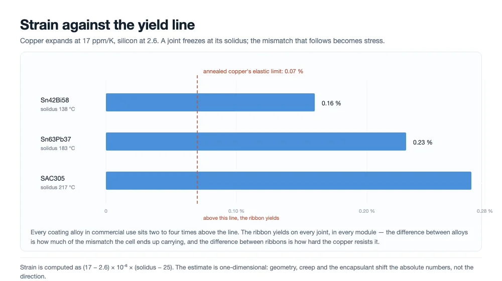
Now compare that with what copper can absorb before it yields. Annealed copper has a yield strength around 80 MPa and a modulus around 110 GPa, which puts its elastic limit near 0.07 percent. Every entry in the table is two to four times that. The ribbon yields on every joint, in every module, on every line — this is not a defect, it is the mechanism. The joint survives because the copper deforms and takes the mismatch onto itself.
Which means the stress the cell carries is set by two things: how much strain the freezing point imposes, and how hard the ribbon resists it. The first is the coating alloy's property. The second is the copper's, and it is the one you can buy. That is why a ribbon specification asks for a yield strength range rather than a maximum softness: soft enough to yield before the cell does, strong enough to survive handling and lamination without sagging.
There is a second thermal cycle that is easy to forget: the laminate. Lamination holds the whole stack at 145 to 160 °C for several minutes. For the solder that means creep, and creep is a partial release of the stress that was locked in at solidification. The ribbon's plastic set does not undo itself and the cell does not get its flatness back, but the joint's residual stress does relax toward whatever the encapsulant allows. Two consequences follow: a module's final bow is set at stringing and only partly softened by lamination, and two lines running identical profiles can produce different modules if their cooling and their stacking before lamination differ.
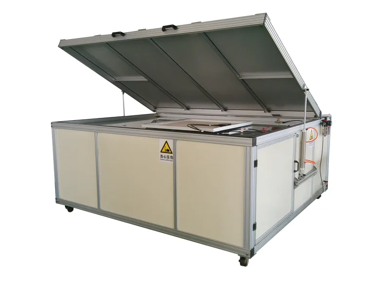
In our laminators, we run this stage between 145 and 160 °C with uniform platen heating, letting the solder joints relieve frozen-in stress without exposing the underlying cell interfaces to uneven thermal gradients across the laminate.
The window therefore has two walls, and they pull in opposite directions. Below it, the coating never clears its liquidus with enough margin, wetting is incomplete, and the joint fails in pull. Above it, the strain and the non-uniformity across the cell climb, and the failure moves from the joint to the silicon. Both walls move with cell thickness: a thinner cell has less thermal mass, bows more for the same gradient, and tolerates a smaller strain before it cracks.
The estimate above is one-dimensional and ignores geometry, creep and how the stack is constrained during lamination. The absolute numbers will shift for a real assembly. The direction and the order of magnitude do not, and they are what make the window narrow.
HJT and back-contact cells narrow it further
Two cell architectures push against the same window from different sides.
Heterojunction cells carry an amorphous silicon passivation stack under a transparent conductive oxide. That stack does not survive a conventional reflow peak, and the practical ceiling for the whole stringing step is usually quoted at or below 200 °C. The two ways around it are a low-temperature coating alloy — SnBi systems, with a solidus near 138 °C — and conductive adhesive cured in the 150 to 170 °C range. Both work. Neither is free: bismuth-bearing joints are less ductile than tin-lead or tin-silver, so a pull strength that looks healthy on day one says little about a joint that will thermal-cycle for 25 years, and adhesive joints trade process simplicity for cost and cure control.
Back-contact cells attack the window from the mechanical side. They are single-sided by construction, so there is no front ribbon counterbalancing the rear one, and at the 240 °C that conventional stringing likes they bow enough to disturb downstream handling. That is the pressure behind tape-based and adhesive stringing for this family, and it is a mechanical problem before it is a metallurgical one: the same joint that would be fine on a double-sided cell is a warpage source on a single-sided one.
0BB moves the joint into the laminator
Busbar cells make the joint at the stringer and inspect it at the stringer. Zero-busbar interconnection breaks both halves of that sentence. Depending on the route, the electrical connection is either made at the stringer with the mechanical bond added by adhesive, or the adhesive holds the wire in place and the actual alloying happens under the laminator. In the third route a single film carries adhesive, cell and wire into the laminator together, and nothing is soldered at all.
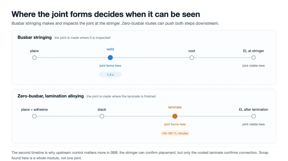
For the ribbon, the consequences are specific rather than philosophical. The coating's solidus stops being a metallurgical detail and becomes a process parameter: in a lamination-alloying route it has to melt inside the lamination window, which for EVA sits around 145 to 150 °C and for POE a little higher. A tin-lead or SAC coating never reaches that, and a low-temperature coating that does has to be matched to the encapsulant, the adhesive and the cell's own temperature ceiling all at once.
When running zero-busbar stacks with EVA, we hold the chamber within that 145 to 150 °C window so the coating reflows and alloys reliably across every wire contact without blistering the encapsulant or misaligning the grid.
The joint area shrinks too. Without a busbar there is no wide pad to forgive a placement error; the contact is where fine wire crosses a finger, and the fraction of that area that actually wets is what carries the current. Finer wire also means the straightness and stiffness specifications tighten, because a wire that wanders is no longer hidden by a 1 mm busbar.
The most expensive change is not in the ribbon at all. It is where the defect becomes visible. A joint formed under the laminator can only be inspected after lamination, when the module is already assembled and the scrap value of a failure is the whole laminate. The stringer stops being the quality screen, and the controls that used to catch problems at the joint have to move upstream — coating thickness, wire placement accuracy, adhesive weight — where they are cheaper per defect but harder to see.
What the stringer keeps, in every route, is placement. The wire has to arrive on the finger with the right spacing and the right tension, and the adhesive has to hold it there through handling into the laminator. That is a different skill from soldering: there is no reflow window to tune, no wetting to watch, and no pull test that can be run on a single joint. The controls are vision, tension and adhesive weight, and the confirmation is an EL image taken after the laminate has cooled.
This is why the zero-busbar transition changes what a ribbon supplier is asked to prove. Under busbar stringing, the ribbon's job could be verified joint by joint. Under lamination alloying, the ribbon, the adhesive and the encapsulant form one system whose behaviour is only visible at the end, and the specification has to be written as a compatibility requirement rather than a set of independent values.
Six defects and what each one is telling you
| Symptom | Usual cause | First thing to check |
|---|---|---|
| Cold joint, low pull strength | Peak too low, flux expired or under-applied, coating oxide | Profile against coating solidus; flux batch date |
| Yellowed, over-soldered joint | Peak too high or dwell too long | Emitter ageing; recent recipe change |
| Microcracks after stringing | Ribbon too hard, pin pressure high, uneven heating | Yield strength of the current ribbon batch; pin force |
| Ribbon off pad, white edge | Camber, placement error | Camber limit against the incoming certificate |
| Solder balls | Coating too thick, peak too high | Coating thickness per side |
| String bow | Thermal mismatch, stiff ribbon, fast cooling | Ribbon softness, cooling rate, cell thickness |
The table is only useful if it is read as an elimination order rather than a diagnosis. Two different causes can produce the same symptom, and the distinguishing evidence is usually cheap: a camber gauge, a pull test on a known-good batch, a cross-section. What makes debugging slow is not the diagnosis itself but changing two levers at once, because the process then has no way to attribute the improvement.
What to put in the ribbon and process specification
Six values cover most of what this article argues. They are worth writing down explicitly because each one maps to a failure mode the line will otherwise discover at 3 a.m.
| Specification | Why it is on the list |
|---|---|
| Yield strength as a range (Rp0.2) | Sets how much of the mismatch strain the ribbon absorbs instead of the cell |
| Coating thickness per side, with tolerance | Drives solder-ball formation and the amount of alloy available to wet |
| Coating alloy and its solidus | Fixes the strain the joint starts from, and the lamination window it can work in |
| Camber and straightness limit | Prevents white-edge and ribbon-off-pad defects that scale with line speed |
| Flux activation window against the profile | Ensures the flux is active before the coating reaches its liquidus |
| Peak and edge-to-centre uniformity | Keeps the coolest strip wetting without over-heating the centre |
If you have to prioritise, the yield strength range and the coating's solidus are the two that change the failure mode rather than the failure rate. A ribbon that is slightly too thick will produce solder balls and be corrected by a tolerance. A ribbon that is slightly too hard produces cracked cells on thin wafers and a scrap event that arrives weeks after the batch was accepted. That asymmetry is worth remembering when a purchasing decision comes down to price per tonne.
Verification belongs on arrival, not on the line. Pull strength, coating thickness, camber and a cross-section cost minutes per consignment; a cracked string costs the cells, the labour and the schedule of whatever module line was downstream of it. The incoming tests are cheap enough that the only real question is whether anyone is scheduled to run them.
Frequently asked questions
At what temperature are solar cells soldered?
With conventional tin-based coatings the peak at the joint is typically 230 to 250 °C, reached in one to two seconds after a preheat near 120 °C. Heterojunction cells cap the step at or below 200 °C, which is why they use low-temperature alloys or conductive adhesive. In zero-busbar routes where the joint forms under the laminator, the alloying happens in the lamination window around 145 to 160 °C.
Why does the ribbon yield during cooling?
Because the mismatch strain is two to four times what copper can absorb elastically. From a tin-lead solidus of 183 °C, the strain to room temperature is about 0.23 percent; annealed copper's elastic limit is about 0.07 percent. The surplus has to become plastic deformation, and that is the intended behaviour — the ribbon yields so the silicon does not.
Is a thicker intermetallic layer a stronger joint?
No. A continuous layer of roughly 1 to 3 micrometres gives the best combination of bond strength and toughness. Thinner than that, the bond is incomplete. Thicker than about 5 micrometres, the interface is brittle and a crack starting there runs along it instead of stopping. Duration at temperature grows the layer faster than it improves the bond.
Can a busbarless cell be soldered on a stringer?
Yes, in routes where the wire is welded at the stringer and adhesive provides the mechanical bond. In the route where adhesive holds the wire and the alloy melts during lamination, there is no solder reflow at the stringer at all. The distinction matters for equipment selection, because the two routes put the process control in different machines.
Why do zero-busbar defects only appear after lamination?
Because in the lamination-alloying route the joint does not exist until the laminate reaches temperature. The stringer only places and holds; the electrical connection forms later. Any inspection before lamination can confirm placement but not connection, which is why upstream controls on coating, adhesive and placement carry more weight than they do on a conventional line.
Does flux residue weaken the joint?
Not directly. Joint strength is set by wetting and the intermetallic layer; residue sitting on the surface does not change either. Residue matters for long-term reliability and for the appearance of the module, which is a different conversation from whether the joint formed.
How do I tell a cold joint from a lifted ribbon?
Look at the fracture surface. A cold joint separates at the alloy-to-grid interface and leaves the grid largely intact, often with a smooth, shiny oxide film visible. A lifted or badly placed ribbon leaves a tear in the grid or pulls grid metal away with it. The two look similar on an EL image and are different problems on the line.
Does a lower peak temperature always extend cell life?
No. Lowering the peak reduces strain and bow, but if it goes far enough to stop the coating from wetting properly, the joint fails mechanically long before the cell would. The optimum is the highest peak that still keeps the strain and the edge-to-centre gradient inside limits, not the lowest peak the machine can hold.
Final thoughts
A ribbon joint is decided in one or two seconds, by four variables the machine controls and six it inherits. The metallurgy sets the floor, the strain sets the ceiling, and the two walls have been moving closer together as cells get thinner, architectures get cooler, and zero-busbar pushes the joint under the laminator. The good news is that the levers are ordinary: a profile matched to the flux, a ribbon with the right yield strength range, and incoming checks that catch a bad batch before it becomes a cracked string.
Related reading:
- Tabber and stringer machine: how it works and how to choose
- Solar cell stringer mechanisms: a zone-by-zone guide
- PV ribbon materials: copper core, hardness and coating
- PV ribbon structure and types: flat, round and shaped
- 0BB cell technology: what removing the busbar changes
- Why is flux essential for photovoltaic soldering
- Solar module stringing: troubleshooting cold solder joints
- PV ribbon test methods: what to verify before production
Sources: thermal profile data from Joseph et al., EPJ Photovoltaics 16, 9 (2025), a validated model of infrared ribbon welding on an industrial stringer; strain figures calculated from published coefficients of thermal expansion for copper and silicon; bow observations at conventional stringing temperatures for back-contact cells as reported by TaiyangNews.
We supply single and double chamber solar panel laminator machines with oil-heated or electric platens to support both standard stringed modules and zero-busbar lamination-alloying schedules. If you are refining your thermal cycle or qualifying new encapsulant recipes, share your module stack, lay-up drawings, or sample materials with our engineering team for an equipment evaluation.