Editorial responsibility for this article rests with Wuhan Ooi Photoelectric Technology Co., Ltd. Written and reviewed by the Ooitech editorial team. See our editorial policy for how we write, where AI tools are used, and how to request a correction.
PV Ribbon Structure and Types: Flat, Round and Shaped
Table of Contents
Quick answer: A PV ribbon is a copper conductor with a solder coating. Interconnect ribbon joins cells into strings and comes in two forms, flat strip and round wire. Busbar ribbon collects the current from those strings and is almost always flat and wide. Round wire displaced flat strip for two reasons: at the same current-carrying section it shades less, and because there are more of them, each one thinner, the cell can print far less silver.
Ribbon is the least glamorous part of a module. It is a copper strip a fraction of a millimetre thick, soldered across every cell, and it decides three things at the same time: how much current reaches the busbar, how much light never reaches the cell, and how much mechanical stress the cell carries once the joint has cooled.
Those three jobs pull in different directions. A thicker ribbon conducts better but shades more; a softer ribbon protects the cell but stretches under stringer tension; a wider busbar lowers resistance but creates a bump under the glass after lamination. Every change in ribbon form over the past decade has been a new balance point between them.
This article covers the shape side of that trade: what a ribbon is made of, how interconnect and busbar ribbon differ, why interconnect ribbon moved from flat strip to round wire, and what the shaped variants are for. The material side — copper grade, coating alloys, coating thickness and intermetallic growth — is covered separately in PV ribbon materials: copper core, hardness and coating.
What a Ribbon Is Made Of
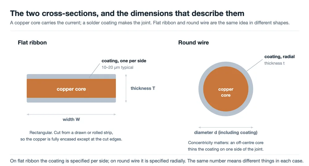
Whatever the shape, the construction is the same: a copper core with a solder coating around it. The two parts have separate jobs.
- Copper core. Carries the current and holds the ribbon together mechanically. It is normally high-purity oxygen-free copper, because resistivity falls as purity rises, and it is annealed to a controlled yield strength so that it does not pull the cell apart as the joint cools.
- Solder coating. Makes the joint. It melts during soldering, wets the cell's gridline, and protects the copper underneath from oxidation. Coating thickness is usually measured in tens of microns.
A reasonable question is why the whole ribbon is not simply copper, or simply tin. Copper does not form a reliable joint with a printed gridline on its own, and it oxidises readily. Tin conducts only about a seventh as well as copper and is too soft to hold a string together. Copper as the frame and tin as the skin is a compromise between conduction, soldering and cost.
The coating looks like a detail and behaves like one of the main variables. Too thin and there is not enough solder to form a full joint, which shows up as a weak pull strength or a dry joint, especially after storage oxidation. Too thick or uneven and the excess solder can spill into beads or bridges during soldering, while the coating consumes cross-section that carries almost no current. On round wire, whether the coating is concentric matters as much as its average thickness: an off-centre core thins the solder on one side of the joint.
Describing a ribbon usually comes down to five parameters, and each one answers to a different role:
| Parameter | What it describes | What it affects |
|---|---|---|
| Width × thickness, or diameter | Cross-section of the conductor | Resistance, shading, mechanical stress |
| Coating composition | SnPb, SnPbAg, SnBi or a lead-free alloy | Soldering temperature, wettability, compliance |
| Coating thickness | Average thickness and its uniformity | Pull strength, risk of a dry joint |
| Resistivity | How well the metal conducts | Resistive power loss in the string |
| Yield strength and elongation | How soft and how ductile the copper is | Microcracks, cell breakage, stretch during stringing |
Two Families: Interconnect and Busbar Ribbon
The first division in the industry is by position in the module, and it is the most useful one to hold on to.
| Interconnect ribbon | Busbar ribbon | |
|---|---|---|
| Also called | Tabbing ribbon, stringing ribbon | Busbar, bus ribbon |
| Position | Front and back of every cell | Ends of the strings, and the leads out of the module |
| Job | Connects cells in series to form a string | Collects string current and carries it to the junction box |
| Form | Thin: flat strip or round wire, ten to twenty-plus per cell | Wide and flat, usually a few millimetres across |
| Rate of change | Fast, it follows cell technology | Slow, driven by cost and thinning |
Interconnect ribbon is where the technical development happens and where the entry barriers sit, which is why most of this article is about it. Busbar ribbon carries the highest current in the module, and the joints at the end of a string and at the lead-out are a well-known location for hot spots and local overheating, so a design that looks unchanged is not a design without risk.
Its recent evolution runs along two lines. The first is thinning: the thicker the busbar, the more pronounced the bump it creates between glass and backsheet after lamination, and the higher the local stress around it. The second is layout adaptation — centre bussing for half-cut layouts, folds that reduce the edge margin, punched or pre-formed leads. Both aim at the same target: save space and copper without adding resistance. Our interconnection busbar page covers the material side of that component.
From Flat Strip to Round Wire: Four Generations
Interconnect ribbon has gone through four recognisable stages, and the direction of travel is easy to describe: more wires, each one thinner.
- 3BB to 5BB. The cell prints three to five wide main gridlines, and the ribbon is a rectangular flat strip, typically 1.5 mm wide in the early days and below 1 mm later on.
- MBB (multi-busbar). The main gridline count rises to nine or twelve, and the ribbon becomes a round wire of roughly 0.3 to 0.4 mm. The current is split over more conductors, and the distance it travels along the fingers before it reaches a wire is shorter, which reduces resistive loss in the cell itself.
- SMBB (super multi-busbar). Sixteen or more gridlines, wire diameter between roughly 0.2 and 0.3 mm. This is the mainstream configuration on TOPCon modules.
- 0BB. No main gridline at all. The wire contacts the fingers directly and is held in place by an adhesive film or a dispensed adhesive rather than soldered to a printed pad. Diameter drops below 0.2 mm and the count can reach twenty or more.
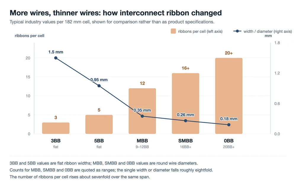
Two forces drive the sequence. The first is silver: a cell with twelve thin gridlines needs far less paste than one with five wide ones, and 0BB removes the main gridline altogether. The second is shading, which the next section deals with.
The manufacturing consequences are less often discussed than the benefits. A round wire touches the gridline along a line rather than across a face, so the joint area of a single wire is small. That puts more weight on soldering temperature, pressure and coating consistency: get them wrong and a wire that looked connected at the stringer shows up as a hot spot later. The stringer has to feed, position and hold sixteen, twenty or more fine wires at once, and one wire that lands off position is either a dry joint or a finger covered by solder. At 0BB the connection is made during lamination rather than at a soldering station, which moves ribbon and film into a single process that has to be qualified together. Straightness, roundness and diameter tolerance all become tighter as the wire gets thinner, and the thinner the wire, the more a small diameter variation matters to the cross-section it is supposed to provide.
That is also where equipment and material have to be matched: the MBB tabber stringer and the ribbon it runs are a pair, and the ribbon drawing and tinning line upstream is where the diameter, straightness and coating uniformity are actually fixed.
Why More Wires Do Not Mean More Shade
The intuitive reading of the previous section is that replacing five flat ribbons with twenty round wires should cover four times as much of the cell. It does not, for two separate reasons.
The obvious one is that the wires are much thinner. On a 182 mm cell, the geometric width covered by the conductors barely changes across the four generations:
| Configuration | Count and size | Geometric shading width | Effective shading |
|---|---|---|---|
| 3BB | 3 × 1.5 mm flat | 4.5 mm | about 2.5% |
| 5BB | 5 × 0.95 mm flat | about 4.8 mm | about 2.6% |
| MBB | 12 × 0.35 mm round | about 4.2 mm | about 1.5% |
| SMBB | 16 × 0.26 mm round | about 4.2 mm | about 1.5% |
| 0BB | 20 × 0.18 mm round | about 3.6 mm | about 1.3% |
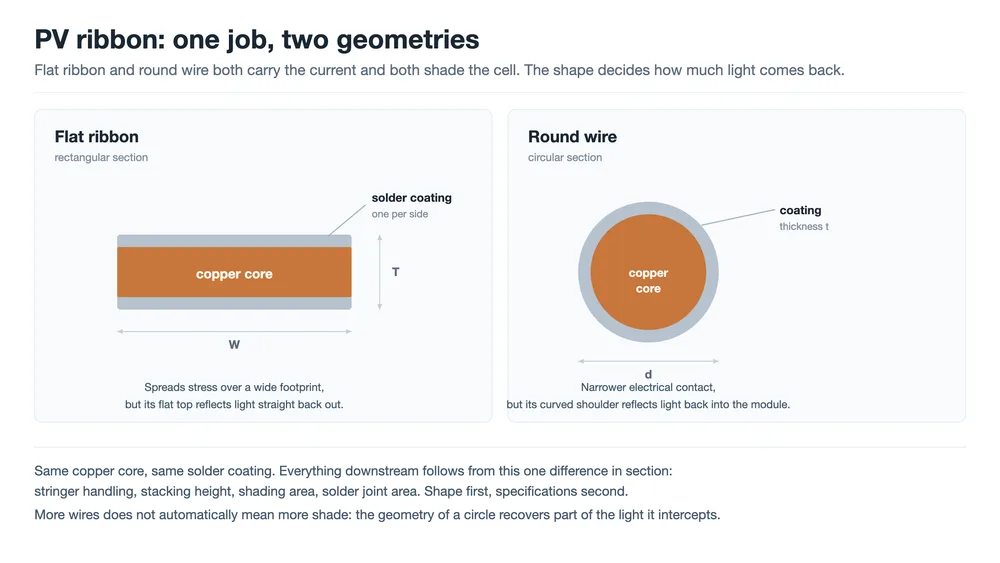
The less obvious reason is the shape. Light that hits the flat top of a rectangular ribbon is reflected straight back out through the glass, and the cell never sees it again. Light that hits the curved shoulder of a round wire leaves at a shallow angle, and at a shallow enough angle the glass-to-air interface reflects it back down onto the cell instead of letting it escape. That second pass is why round wire shades less than its geometry suggests.
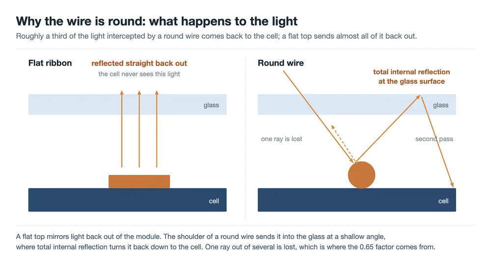
In practice the industry accounts for this with an effective shading coefficient: 1.0 for flat ribbon, and roughly 0.65 for round wire, which implies that about a third of the light intercepted by a round wire makes it back to the cell. Put those coefficients against the table above and the whole evolution makes sense. From 3BB to 0BB the ribbon count rises roughly sevenfold while the single ribbon dimension falls roughly eightfold, the geometric shading width stays close to 4 mm, and effective shading falls from about 2.5% to about 1.3%. More wires, less shade.
Two caveats belong with those numbers. They are calculated on a 182 mm cell for comparison, while the 3BB and 5BB era mostly used smaller cells, so the early figures would shift a little on an older format. And the recovery from total internal reflection depends on the glass, the encapsulant and the angle of the incoming light, so the 0.65 coefficient is a working estimate rather than a constant.
Shaped Ribbons: Triangular, Segmented and Reflective
Once shading became the constraint, ribbon geometry itself became a design variable. Four variants are in use, and each one solves a specific problem.
- Triangular ribbon. A flat base sits on the gridline and the apex points up, so the two sloped faces reflect incoming light sideways instead of straight back. The contact face stays flat, which keeps the joint area that a round wire gives up.
- Segmented ribbon. One continuous ribbon with a different section along its length — round where it crosses the front of a cell, flattened where it lands on the back of the next one, with a transition at the step between them.
- Flat-round. A compromise section that keeps part of the curved reflective shoulder while widening the contact area.
- Reflective ribbon. Flat strip with fine V-grooves rolled into the surface, which turns a flat top into many small sloped reflectors.
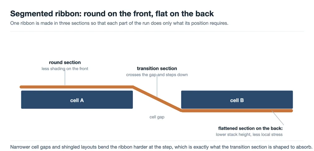
Segmented ribbon is the one that follows directly from module layout. As cell gaps get narrower and shingled layouts overlap cells, the step the ribbon has to cross becomes sharper, and a single uniform section has to compromise between the two sides. Allowing the front section to be round and the back section to be flat gives each position the shape it needs. The cost is that the ribbon is no longer a simple extrusion, tolerances tighten along the length, and the stringer has to place it with the transition in the right spot.
Different Cells, Different Ribbons
Ribbon selection follows cell technology, because the cell decides the electrode pattern, the soldering temperature it can survive, and whether the front side is shaded at all.
| Cell technology | What it asks of the ribbon | Typical choice |
|---|---|---|
| PERC | Conventional soldering temperature, mature process | Standard coated round wire, MBB or SMBB counts |
| TOPCon | Bifacial, finer and denser fingers | SMBB round wire, shaped ribbon, 0BB being introduced |
| HJT | Amorphous silicon and the transparent conductive layer are temperature sensitive | Low-temperature coating, or 0BB interconnection through a film |
| BC | Both polarities sit on the back; the front carries no ribbon | Rear-side ribbon, placed to avoid shorting the two polarities |
The low-temperature family exists because of HJT. A conventional tin-lead coating melts around 183 °C; the tin-bismuth eutectic systems used for temperature-sensitive cells melt at roughly 139 °C. Lower soldering temperature means less thermal stress on the cell, which is why the same approach has spread to thin wafers beyond HJT: the reason is not only the cell structure but the fragility of the wafer.
Back-contact cells reverse the priority. With no ribbon on the front, shading no longer limits the width, so the ribbon can be wider and flatter to cut resistance, which is the opposite of what a front-side interconnect wants. What replaces shading as the constraint is alignment: two polarities of opposite sign sit close together on the same face, and a ribbon that bridges them is a short circuit. The rear-side geometry usually needs an insulation scheme or a shaped section to keep the two apart.
Beyond those four, ribbon is also sold by appearance and by compliance. Black ribbon is used in full-black modules where a bright silver grid would spoil the finish, and lead-free coatings appear where substance restrictions are strict. In both cases the difference is in the coating and the surface, not in the structure of the conductor, and both change the soldering window, so they have to be validated rather than assumed.
How to Choose: Four Questions
Ribbon is often specified by copying the previous module. Working through four questions first tends to produce a better answer.
- Which cell technology? This sets the coating system and the soldering temperature. HJT and thin wafers push towards low temperature; BC depends on the rear electrode layout and the insulation scheme rather than on shading.
- What does the gridline design look like? The number of main gridlines fixes the ribbon count and diameter. If the answer is 0BB, the film or adhesive becomes part of the decision, and ribbon and auxiliary material have to be qualified together rather than one after the other.
- What does the layout constrain? Narrower cell gaps and shingled arrangements call for segmented or flattened sections that let the ribbon release stress at the step. Around the busbar, look at the busbar thickness and how it folds.
- Who is the module for? A full-black rooftop module may need black ribbon; a market with strict substance rules needs the lead-free soldering window investigated before the order, not during the first production run.
Only after those four are settled does it make sense to compare diameter tolerance, yield strength, coating uniformity and price. Compared the other way round, the specification ends up driven by whichever data sheet is easiest to read.
Frequently Asked Questions
What is the difference between interconnect ribbon and busbar ribbon?
Interconnect ribbon joins individual cells into a series string and sits on the front and back of every cell. Busbar ribbon collects the current from those strings and carries it to the junction box, and it sits at the ends of the strings. Interconnect ribbon is thin and numerous, busbar ribbon is wide and flat and few. Most of the technical development happens in the interconnect group.
Why did modules switch from flat ribbon to round wire?
Two reasons that reinforce each other. A round wire reflects intercepted light at a shallow angle, so part of it is totally internally reflected at the glass surface and reaches the cell on a second pass, which a flat top does not do. And because more, thinner wires carry the same current, the cell can be printed with many narrow gridlines instead of a few wide ones, using less silver paste.
Do more wires shade the cell more?
No, and the numbers are counter-intuitive. On a 182 mm cell the geometric width covered by the conductors stays near 4 mm from 3BB to 0BB, because the count rises about sevenfold while the single dimension falls about eightfold. Adding the shape effect, effective shading falls from roughly 2.5% to roughly 1.3% over the same span.
What is a segmented ribbon for?
It changes section along its length, so the part crossing the front of a cell can be round while the part landing on the back of the next cell is flattened. Narrow cell gaps and shingled layouts make the step between cells sharper, and a single uniform section would have to compromise between the two positions.
Which ribbon do HJT cells need?
A low-temperature ribbon, usually with a tin-bismuth coating that melts near 139 °C instead of the 183 °C of a conventional tin-lead coating, or an interconnection scheme that avoids soldering altogether. The cell's amorphous silicon layers and transparent conductive layer set the temperature ceiling, so the soldering window is defined by the cell rather than by the ribbon.
Is round wire harder to solder than flat ribbon?
The joint is smaller because the wire touches the gridline along a line rather than across a face, so the process window for temperature, pressure and contact time is narrower and coating consistency matters more. That is a process question rather than a property of the wire: the same machine settings that suit a flat strip will not automatically suit a 0.26 mm round wire.
Final Thoughts
The shape of a ribbon is decided by the cell it connects, and the direction of change has been consistent for a decade. More gridlines means thinner conductors; thinner conductors means round rather than flat; temperature-sensitive cells means lower melting points; electrodes moved to the back means shading stops being the constraint at all.
What does not change is the trade behind the shape. Every ribbon has to conduct without losing measurable power, shade as little as possible, and survive the thermal cycle of soldering without cracking the cell underneath. Whichever generation is on the line, those are the three numbers to check, and the material behind them is where most of the remaining gap between suppliers sits.
Related: PV ribbon test methods: dimensions, strength and solderability. The dimensional checks differ by form; this page covers both flat and round.
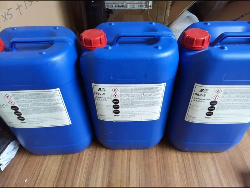
Related reading: PV ribbon materials: copper core, hardness and coating · PV ribbon machine: wire drawing and tinning line · PV busbar ribbon production line · PV ribbon and flux · Busbar welding in module manufacturing
Shading figures are calculated on a 182 mm cell with a uniform incident spectrum, using an effective shading coefficient of 1.0 for flat ribbon and 0.65 for round wire, and are given for comparison between configurations rather than as specifications of any product. Ribbon counts and dimensions from 3BB to 0BB are typical industry values and are commonly quoted as ranges. Power-loss figures for resistive heating are not included here.
This article describes ribbon configurations and their process implications in general terms. For a specific module design, the ribbon, flux and soldering parameters need to be evaluated together on the actual line.
Flat vs round ribbon: why BC cells break the rule — the same four generations, seen from a back-contact cellRelated: What a PV ribbon does: three jobs, one trade-off frames the same geometry in terms of the three roles the ribbon has to serve.
Related: How PV ribbon is made: drawing, annealing and tinning is the product-side view of what those process settings have to produce.