Why Does Electrifying a Solar Panel Reveal Hidden Cell
Table of Contents
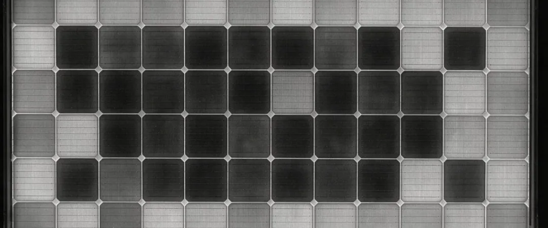
Quick answer: Electrifying a solar panel and photographing its own emission reveals defects that no visual inspection can find. In electroluminescence testing, current is injected into the module so the cells emit infrared light, and a camera images that emission at wavelengths around 1150 nm. A crack, a finger interruption or a soldered joint with poor contact shows up as a dark feature because less current flows there and less light is emitted. The reason this matters is that these defects are invisible to the eye and often barely visible in a power measurement: a module with a cracked cell can still produce close to its rated output while carrying a defect that will grow. That is why EL testing sits alongside flash testing rather than replacing it — one measures output, the other finds where the output is hiding.
PV Module Manufacturing · by Jerry, Ooitech
Before leaving the factory, solar panels go through two major quality checks. One is a simple visual inspection. The other is what we're talking about today: the power-on test. The technical name for this is the EL test. EL stands for Electroluminescence.
1. The Science Behind EL Testing
A crystalline silicon solar cell is essentially a PN junction semiconductor. It has bidirectional photoelectric properties. In our daily use, sunlight hits the panel, triggers the photovoltaic effect, and turns light energy into electricity.
EL testing flips this physical process backward. An external power source applies a forward direct current to the module. This injects electrons and holes into the cell. These charge carriers recombine at the PN junction and release energy as photons, creating the electroluminescence effect.
Here is the catch. When the silicon cell gets powered, the light it emits is near-infrared, with a wavelength around 1100-1150nm. This specific band falls completely outside human vision. We can't perceive this light at all. Even if the module is fully powered and glowing, it just looks like a regular piece of glass to the naked eye. You won't see any bright or dark patterns.
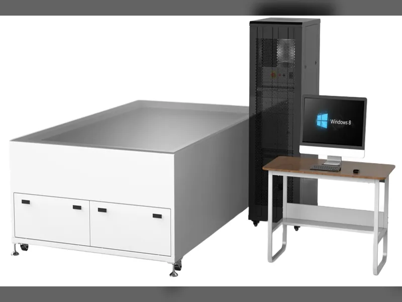
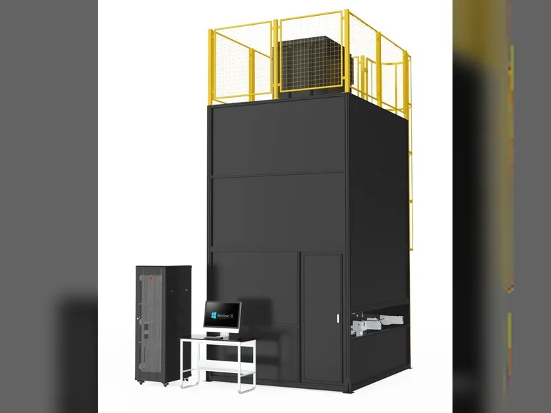
That is why just applying power is nowhere near enough. We have to rely on specialized infrared imaging cameras. EL equipment uses near-infrared sensitive CMOS or CCD cameras paired with IR filters. They take long-exposure shots in a completely dark environment. This setup converts the invisible infrared signals into clear black-and-white images on a monitor.
2. Why Do We Need EL Testing?
Think of it as a CT scan for solar panels. Defects you cannot spot from the outside become crystal clear through an EL test. Let's look at a few common EL defects: micro-cracks, cold soldering, and broken grid lines.
Micro-cracks:These are micro-fractures in the silicon body caused by mechanical stress. The cell hasn't completely snapped apart, so the surface looks fine. But the crystal lattice is already cracked. Since it is actual damage to the silicon base, the EL camera catches it easily. In an EL image, a micro-crack shows up as a distinct black line.
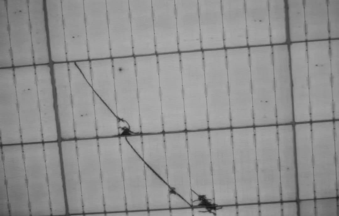
Cold Soldering:This happens when a good alloy contact fails to form between the soldering ribbon and the cell's main busbar. They touch mechanically, but the electrical connection is weak. In EL images, cold soldering appears as local dark spots or dark lines. You will usually see them running along the grid lines, showing up as irregular, broken black lines or dotted patches.
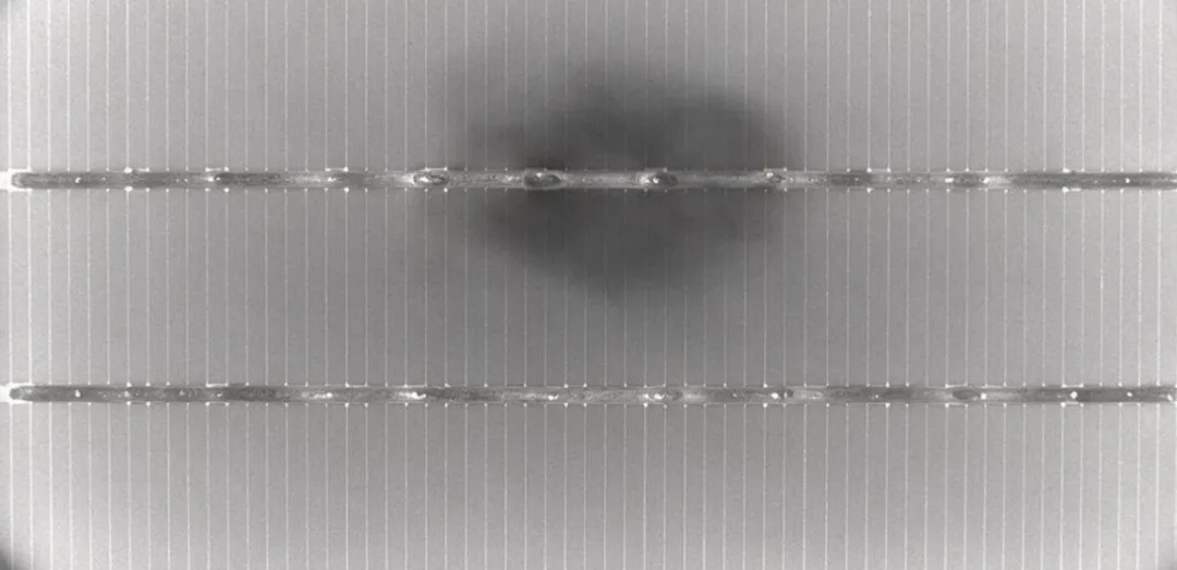
Broken Grid Lines:Sometimes the fine silver grid lines on the cell break. When this happens, the current collection path gets cut off. This is almost always a raw material defect. You can spot it in an EL scan as black or dark areas running perpendicular to the main busbar.
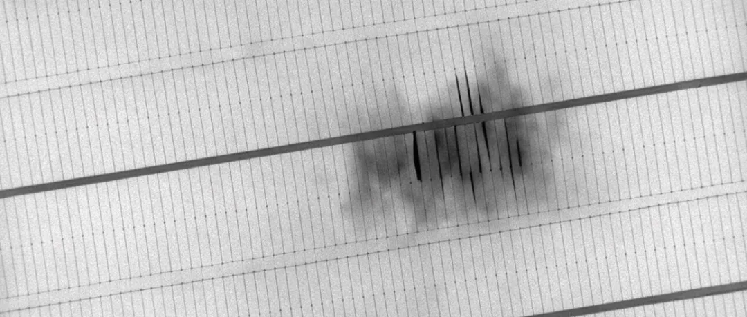
About 15 years ago, buyers rarely asked for EL inspections. Today, it is an absolute must-have for panel shipments, tested at 100% capacity on the line. Things like micro-cracks, cold soldering, and broken grids will seriously drag down a module's power output and ruin its long-term reliability.
Ooitech's View
Quality control hardware has drastically evolved to keep pace with modern high-efficiency cell architectures like TOPCon and HJT. Pushing panels through EL testers isn't just about catching defects anymore; it's about fine-tuning the upstream tabber stringer and laminator parameters in real time. Factory yields jump significantly when EL data directly feeds back into the production line's main control system to prevent repeated mechanical stress issues.