Why Metallization Sets the Efficiency Ceiling
Table of Contents
Quick answer: Metallisation is the ceiling on efficiency for high-efficiency solar cells, because it has to do two contradictory jobs at once. The silver fingers must be wide enough to carry current with low resistance, and narrow enough to block as little light as possible. Every improvement in cell efficiency makes that tension tighter, because a higher-current cell loses proportionally more to series resistance in the same finger geometry. The process side is equally constrained: contact formation involves a firing step in the region of 800 °C, and the paste chemistry that makes a good ohmic contact at that temperature also interacts with the emitter beneath it. Silver paste is the largest non-silicon cost in the cell, which is why the industry keeps pushing finger width down and why the search for a cheaper contact material has run for years.
PV Module Manufacturing · by Jerry, Ooitech
Why Metallization Sets the Efficiency Ceiling for High-Efficiency Solar Cells
In the broader story of photovoltaic technology, every small gain in conversion efficiency usually comes from pushing microscopic physical limits a little harder. Since the industry moved beyond the monocrystalline PERC era and began shifting toward N-type technologies such as TOPCon, HJT, and BC, the efficiency ceiling has continued to rise.
As solar cells move closer to the Shockley–Queisser limit, one of the most basic yet difficult problems in semiconductor physics becomes increasingly important: the electrical contact between a metal and a semiconductor. This interface has become a core technical barrier affecting mass-production yield and final cell efficiency.
To a non-specialist, a solar cell may look like a thin semiconductor wafer that simply generates electricity under sunlight. From an industrial and academic point of view, however, it is a highly precise quantum-mechanical energy conversion device. It must separate the electron-hole pairs generated by absorbed photons and guide them into an external circuit with as little loss as possible.
During this process, the metal electrodes act like toll stations where charge carriers leave the microscopic semiconductor world. If a large barrier exists at the station, carriers become congested, recombine, and lose energy. At the device level, this appears as a sharp increase in contact resistance, a steep drop in fill factor, and ultimately a reduction in solar-cell output power.
The ability to form a low-resistance ohmic contact on a surface that must also maintain extremely low recombination has therefore become a critical dividing line for modern high-efficiency solar cells.
Ohmic Contact: Bridging the Physical Gap Between Metal and Semiconductor
To understand the metallization problem, we first need to return to semiconductor band theory. This includes the built-in electric field inside a semiconductor and the microscopic charge transfer that occurs when a metal meets a semiconductor.
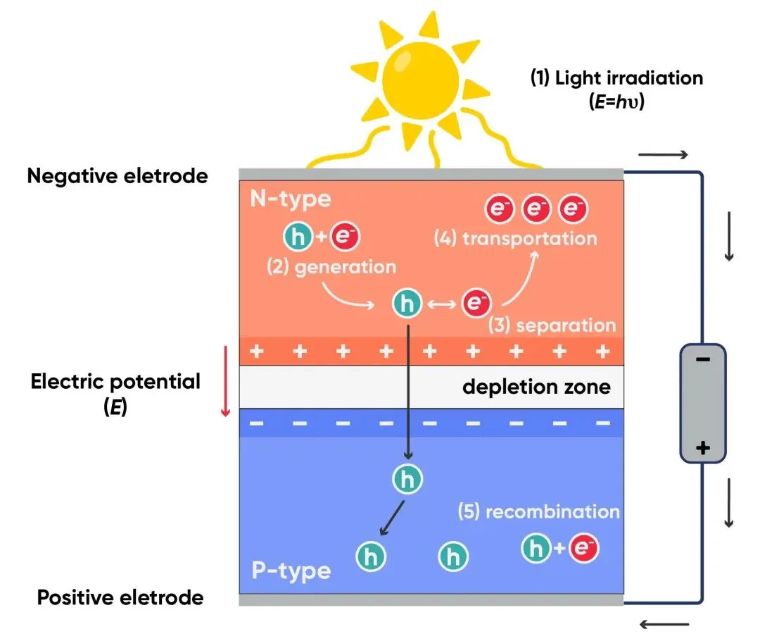
The physical basis of photovoltaic conversion is the PN junction. When P-type and N-type semiconductors with different doping concentrations come into contact, their Fermi levels are different. To reach thermodynamic equilibrium, microscopic charge transfer takes place.
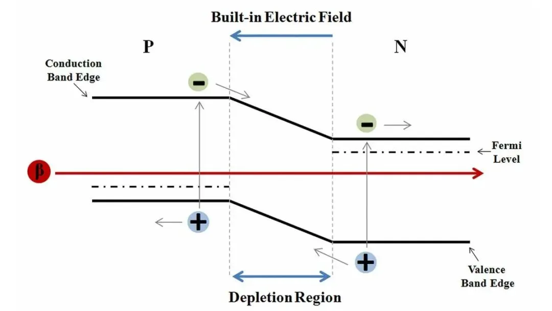
The Fermi level of an N-type semiconductor is higher than that of a P-type semiconductor. Electrons therefore move spontaneously from the N-type region toward the P-type region, while holes move in the opposite direction. As these carriers move, fixed charged ions are left near the PN-junction interface. This creates a space-charge region, also called the depletion region, together with a built-in electric field.
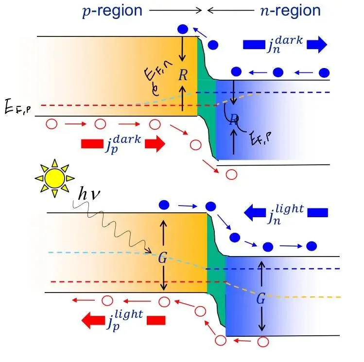
The built-in field bends the semiconductor energy bands and produces a drift force opposite to the direction of carrier diffusion. When diffusion and drift reach dynamic equilibrium, the Fermi levels on both sides align and the net current becomes zero. Under illumination, photogenerated electron-hole pairs are separated by this built-in field, producing a photovoltage and an output current.
This delicate physical process only works efficiently if carriers can leave the semiconductor and enter the metal electrodes without facing another major obstacle.
Schottky Barriers: A High Wall in the Current Path
When a current-collecting metal electrode comes into physical contact with a semiconductor, differences in work function cause charge transfer and band bending at the interface.
Consider a metal in contact with an N-type semiconductor. If the metal work function is greater than the semiconductor work function, electrons at the semiconductor surface move toward the metal. A depletion layer with fewer majority carriers then forms near the semiconductor surface. The energy bands bend upward, creating an interfacial energy barrier known as a Schottky barrier.
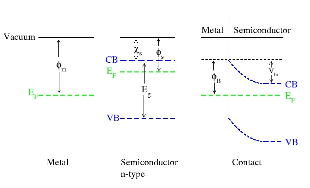
A Schottky barrier has a pronounced rectifying effect, similar to the one-way conduction of a diode. To cross it, carriers in the semiconductor need enough thermal energy to pass over the barrier through thermionic emission.
If a typical Schottky contact forms between the electrode and the silicon substrate of a working solar cell, photogenerated carriers face strong resistance as they move toward the metal. The barrier not only restricts current flow. It also causes carriers to accumulate and recombine at the interface, directly reducing conversion efficiency.
An ohmic contact is the opposite. It is a non-rectifying electrical contact between a metal and a semiconductor, with very low contact resistance. In the ideal case, current passes through the interface linearly in both directions, with minimal voltage drop and energy loss.
In theory, selecting a metal with a very low work function for an N-type semiconductor, or a very high work function for a P-type semiconductor, can help avoid a Schottky barrier. Real silicon surfaces are more complicated. Dangling bonds caused by lattice termination and a high interface-state density can produce strong Fermi-level pinning. Changing the metal work function alone is therefore rarely enough to create a perfect ohmic contact.
The mainstream industrial solution is heavy doping combined with quantum tunneling. A highly doped N++ or P++ layer is formed locally where the semiconductor contacts the metal. This sharply narrows the depletion region at the surface. Once the barrier becomes sufficiently thin, carriers no longer need to pass over it. They can tunnel directly through it with a high probability. This is the quantum tunneling effect.
When Contact Resistance Rises, Fill Factor Falls
Once the physical basis of an ohmic contact is clear, the next question is why the solar industry is so sensitive to microscopic contact defects. The answer involves three key electrical parameters: contact resistance, series resistance, and fill factor.
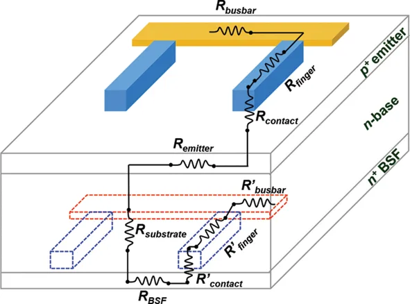
A solar cell is not an ideal current source. It contains several unavoidable resistance-loss mechanisms, collectively represented by series resistance. Series resistance includes the bulk resistance of the silicon wafer, emitter sheet resistance, contact resistance at the metal-semiconductor interfaces, the ohmic resistance of fingers and busbars, and the physical resistance of ribbons and other interconnection materials.
As monocrystalline silicon growth has matured, conductive silver pastes have improved, and screen-printing meshes have become finer, wafer resistance and metal-grid resistance have already been reduced to relatively low levels. In current N-type high-efficiency cells, one of the most difficult microscopic bottlenecks is contact resistance between the metal electrode and the silicon-based contact structure.
If quantum-tunneling-dominated ohmic contact is not established, contact resistance can rise exponentially and become the dominant source of series-resistance loss.
Fill factor is one of the most important parameters used to evaluate solar-cell output and internal energy loss. It is the ratio of the maximum output power to the product of open-circuit voltage and short-circuit current. On an I-V curve, it reflects how square or full the curve appears.
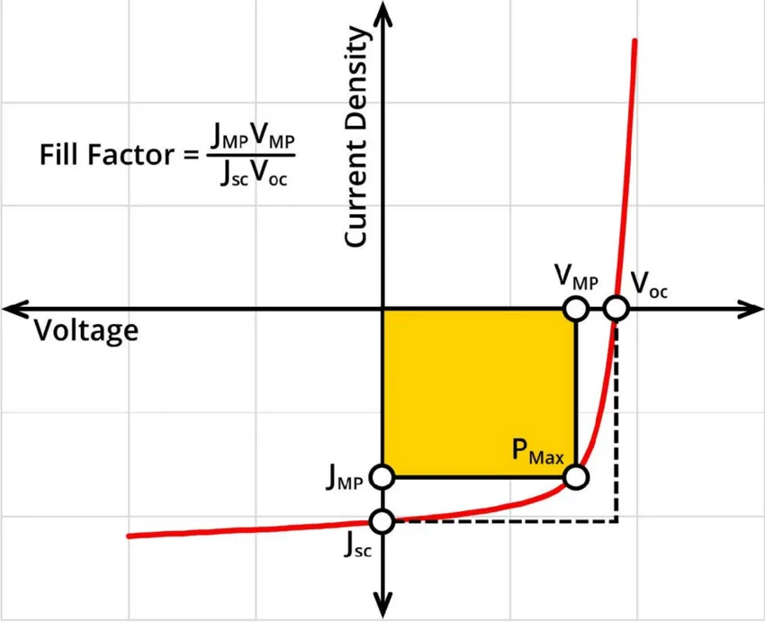
When poor contact causes the ohmic contact to fail, the increase in contact resistance pushes total series resistance sharply upward. The I-V curve then tilts and collapses around the maximum power point. The cell may still show a relatively normal open-circuit voltage and short-circuit current, but the maximum power available to the external circuit can fall substantially.
The technical chain is straightforward:
A poor metal-semiconductor interface prevents a proper ohmic contact.
The failed contact causes interfacial contact resistance to rise.
Contact resistance pushes up total cell series resistance.
High series resistance reduces fill factor.
Lower fill factor pulls conversion efficiency below the mass-production acceptance threshold.
Passivation and Contact: The Built-In Contradiction of Modern Solar Cells
Modern high-efficiency cell design faces a physical contradiction between passivation and electrical contact. To obtain a high open-circuit voltage, engineers need dielectric films that passivate the silicon surface as completely as possible.
Passivation works in two ways. Chemical passivation uses elements such as hydrogen to saturate dangling bonds at lattice defects in crystalline silicon, reducing defect-assisted recombination. Field-effect passivation creates a strong electric field at the interface. Electrostatic repulsion keeps minority carriers of a similar charge away from the surface, cutting off an important surface-recombination pathway.
On the P-type rear surface of a PERC cell, for example, an aluminum oxide film containing a high density of negative charges can create strong band bending and provide both chemical and field-effect passivation. Yet this highly effective insulating dielectric film also becomes an obstacle to current extraction.
To collect photogenerated carriers, metal electrodes still need an electrical path to the silicon substrate. Conventional PERC processing uses lasers to ablate small openings in the rear passivation layer so that aluminum or silver paste can contact the silicon. Direct metal-silicon contact, however, creates intense interfacial recombination. These contact points can behave like recombination sinks.
In the N-type era, where cell development is moving closer to the 29.43% theoretical efficiency limit cited for crystalline silicon, recombination losses from local contact openings become much harder to accept. TOPCon, HJT, and BC technologies must therefore solve the same central problem: how to achieve low-resistance, large-area carrier transport without destroying surface passivation.
TOPCon: Tunnel Oxide and the Microscopic Surgery of LECO
Strong photovoltaic demand has accelerated the replacement of P-type PERC by N-type technologies. According to the industry figures cited here, N-type TOPCon held only about 23% of the cell market in 2023. Its share rose to more than 60% in 2024, while some equipment-coverage data from leading manufacturers indicated an N-type share as high as 71.1%.
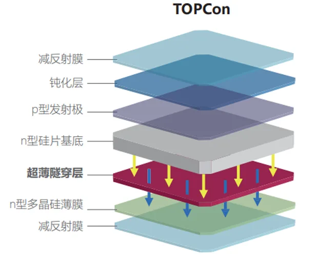
TOPCon retains a high level of compatibility with existing PERC production lines. An upgrade generally requires four additional core processes. The cited equipment investment is around RMB 50–70 million per GW, compared with roughly RMB 350–400 million per GW for a new HJT line. TOPCon also offers clear performance gains over PERC. Its theoretical efficiency limit is reported at approximately 28.7%, while current mass-production efficiencies have commonly moved beyond 26.5% and laboratory efficiencies have exceeded 27.5%.
The key to TOPCon performance is its rear passivating-contact structure. An ultrathin silicon oxide layer is grown on the N-type silicon substrate, with thickness tightly controlled at about 1–2 nanometers. A roughly 60–100 nanometer intrinsic polysilicon layer is then deposited and heavily phosphorus-doped through a high-temperature process.
From the perspective of band physics, the ultrathin silicon oxide layer chemically saturates dangling bonds at the wafer surface. The heavily doped polysilicon produces strong band bending near the interface. This structure creates a high barrier for minority carriers, which are holes in this case, and a much smaller effective barrier for majority carriers, which are electrons. Because the oxide is extremely thin, electrons can tunnel through it into the polysilicon layer, while holes are blocked. The result is carrier-selective transport.
Academic discussions of transport through the oxide include both direct quantum tunneling and the pinhole model. When tunnel-oxide thickness exceeds about 2 nanometers, tunneling probability falls exponentially. Carrier transport may then depend more heavily on microscopic defects or pinholes created during high-temperature annealing. Too few pinholes can raise contact resistance. Too many can indicate extensive film damage and weaken chemical passivation.
Even with a passivating rear contact and a selective emitter on the front, TOPCon faces a serious contradiction during metallization firing. The cell needs high-temperature firing so the silver paste can form a low-resistance contact with the polysilicon. If firing is too aggressive, silver crystallites may penetrate the 1–2 nanometer tunnel oxide and reach the crystalline silicon substrate. The passivation structure can then collapse, dark current can increase, and open-circuit voltage can fall sharply. If the firing temperature is too low, the silver paste may fail to connect properly with the polysilicon. Contact resistance then becomes excessive and fill factor can collapse.
Laser Enhanced Contact Optimization, or LECO, was introduced to address this firing window. The process first uses a specially formulated, less corrosive silver paste. Conventional firing allows the electrode to penetrate the silicon nitride layer without seriously damaging the ultrathin tunnel oxide underneath. After firing, the cell surface is exposed to a high-intensity laser of a selected wavelength while a bias voltage is applied across the electrodes.
Through the photoconductive effect, the local electric field generates a short, high-intensity microscopic current at the metal-semiconductor interface. This pulse behaves somewhat like microscopic lightning. It locally breaks through residual interfacial barriers and creates electrothermal melting and highly localized conductive regions. Numerous small current paths are formed.
After LECO treatment, macroscopic contact resistance can fall by orders of magnitude and a more effective ohmic contact is established. The breakdown is brief and localized. It improves current transport while preserving most of the tunnel-oxide passivation structure.
HJT: A Gentle Contact Between Low-Temperature Silver Paste and TCO
If TOPCon walks a tightrope at high temperature, heterojunction technology operates under a strict low-temperature limit. HJT was first proposed by Japan's Sanyo in the late 1980s. It uses ultrathin intrinsic hydrogenated amorphous silicon films on both surfaces of an N-type crystalline silicon wafer for double-sided passivation. Doped P-type and N-type amorphous silicon layers are then deposited to form the heterojunctions. Its theoretical efficiency limit is generally estimated at around 28.5%, making it one of the leading long-term cell architectures.
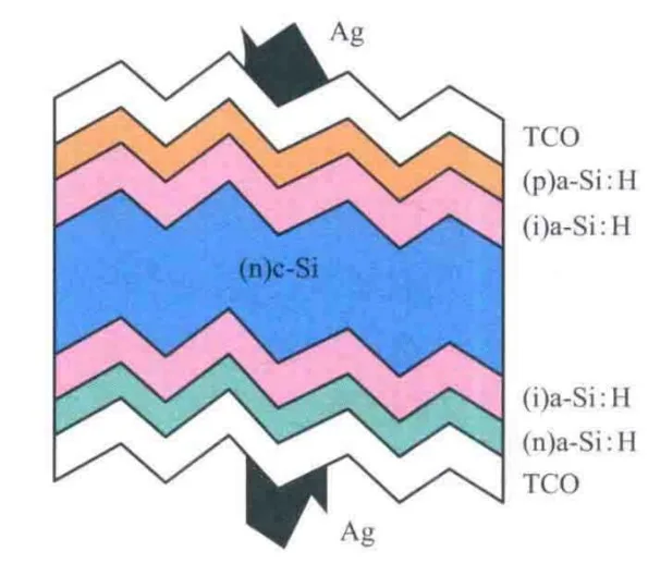
HJT's strong passivation is rooted in the intrinsic amorphous silicon films. Amorphous silicon contains many hydrogen-related Si-H bonds. Hydrogen can saturate dangling bonds on the crystalline silicon surface and provide strong chemical passivation. These bonds are also fragile. Once later processing temperatures exceed roughly 200–250°C, hydrogen can escape from the amorphous silicon film. This dehydrogenation damages the chemical passivation effect.
The temperature restriction has a decisive impact on HJT metallization. Conventional high-temperature silver paste used for PERC and TOPCon, which normally requires firing above 800°C, cannot be used. HJT requires a dedicated low-temperature silver-paste system.
Instead of relying on a high-temperature glass-frit reaction, low-temperature paste uses an organic polymer resin as the binder for conductive silver particles. After screen printing, the cell enters a curing oven operating below approximately 200°C and remains there for a relatively long low-temperature curing cycle.
Solving the temperature problem creates another issue: electrical conduction. Amorphous silicon offers excellent passivation, but its lateral conductivity is poor. After carriers pass through the heterojunction, they cannot travel efficiently over long distances across the amorphous silicon surface to reach the metal fingers.
A transparent conductive oxide film is therefore deposited on top of the doped amorphous silicon, usually by magnetron sputtering. ITO is a common choice. The TCO film transmits light, provides relatively low contact resistivity, and conducts carriers laterally toward the grid lines.
In the HJT stack, the final metallized contact is formed between the cured low-temperature silver paste and the TCO film. This introduces two series-resistance challenges.
First, low-temperature paste depends on shrinkage of the polymer resin during curing. The shrinkage presses silver particles together and against the TCO surface. This physical particle-to-particle contact has significantly higher resistance than the metallurgical bonding produced by high-temperature firing.
Second, the TCO work function must be compatible with both the underlying doped amorphous silicon and the metal electrode above it. Slight oxidation or Fermi-level pinning can create a small Schottky barrier at the TCO-silver interface. That barrier increases series resistance and lowers fill factor.
Paste suppliers are responding by optimizing silver-particle shape, particle-size distribution, and organic resin systems. The HJT industry is also exploring silver-free copper electroplating to move beyond the cost and physical-contact limitations of low-temperature silver paste. Electroplating can grow dense, pure copper grid lines directly on the TCO or on a dedicated seed layer, creating a low-resistance metallurgical contact that is much closer to the ideal state.
BC: A Micrometer-Scale Dance of Rear Electrodes
Within the range of solar-cell architectures, back-contact technology is highly attractive but difficult to manufacture. BC is not one specific substrate material. It is an architectural concept, with the interdigitated back-contact cell, or IBC, as its basic form.
Whether it uses a P-type wafer, a TOPCon-based contact structure, or an HJT structure, the core principle is the same: the emitter, back-surface field, and all positive and negative metal grid lines are moved to the rear of the cell.
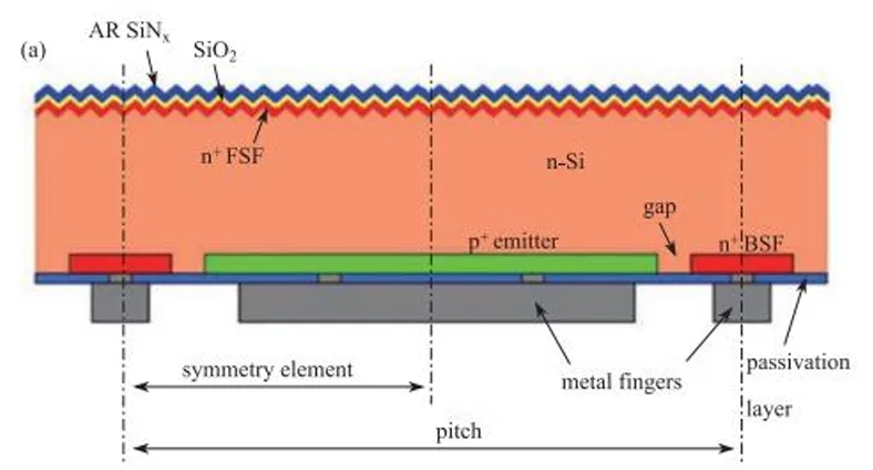
Removing all electrodes from the illuminated surface creates a clear optical benefit: zero front-side metal shading. With no fingers or busbars blocking incoming light, more photons can enter the cell. Compared with conventional bifacial cells, the short-circuit current density of a BC cell can increase by approximately 7%.
At the module manufacturing and encapsulation stage, BC cells can replace the traditional Z-shaped front-to-rear interconnection path with a flat rear-side connection. This reduces mechanical stress between the front and rear surfaces and can improve resistance to microcracks. For example, the edge stress of LONGi HPBC cells has been reported to be 48% lower than that of conventional non-BC cells, supporting improved long-term reliability.
The front-side optical gain has to be paid for through a much more complex rear-side electrical design. On the limited rear surface, the P-type emitter regions and N-type back-surface-field regions are arranged in densely alternating fingers. Separate electrodes must be formed with high precision. The positive metal must create an ohmic contact with the heavily doped P-type region, while the negative metal must contact the heavily doped N-type region.
Three engineering problems stand out.
First, because the front surface no longer collects current, all photogenerated carriers must move through the wafer thickness and then travel laterally in three dimensions toward the appropriate rear contact. If the spacing between positive and negative rear electrodes is too wide, carrier transport paths become longer. Recombination probability rises and lateral bulk resistance increases.
Second, shortening the lateral transport distance requires very tightly spaced positive and negative electrodes. Laser opening combined with screen printing, or insulating-mask and photolithographic metallization, must be aligned with micrometer-level precision. A slight paste overflow or a laser-opening deviation of only a few micrometers can connect the P-side and N-side metals directly, causing severe shunting.
Third, all positive and negative contacts are concentrated in local regions on the rear surface. The total effective metal-semiconductor contact area may be smaller than that of a conventional cell using contacts on both sides. As photogenerated current converges into these local contact points, current density becomes very high. Even a small contact defect can be amplified into a significant resistive and thermal loss.
The Endgame: From Optical Capture to Carrier Management
The industry's focus on ohmic contact and contact resistance reflects a deeper shift in photovoltaic development. The priority is moving from macroscopic photon capture toward precise control of microscopic carrier dynamics.
During the decade dominated by PERC, much of the research effort focused on increasing rear optical reflectance and improving passivation with materials such as aluminum oxide. In the N-type era, advances in materials science have pushed surface chemical passivation closer to its practical limit. The weakest link has moved. Selective carrier extraction and interfacial transport now play a larger role in determining final performance.
The companies and technology platforms that solve metal-interface contact resistance more effectively can build a meaningful efficiency and cost advantage through lower series resistance and higher fill factor.
TOPCon's rapid market expansion in 2024 was not driven only by compatibility with existing PERC lines. Equipment manufacturers and paste suppliers also improved laser-assisted contact processes such as LECO, using localized electrical and thermal effects to balance tunnel-oxide passivation against low-resistance alloyed contact formation.
Looking further ahead, persistently high silver costs and the physical resistance limitations of low-temperature silver paste are pushing silver reduction and copper plating into focus. Electrochemical growth of dense copper on a conductive film or seed layer can create a near-metallurgical ohmic contact while also reducing the electrical resistance of the grid itself.
Final Battle at the Micrometer-Scale Interface
Solar cells are so sensitive to poor contact because the electrode interface is the last and most difficult step in the photovoltaic energy-conversion loop.
TOPCon balances firing conditions against the integrity of a tunnel oxide only 1–2 nanometers thick, with LECO acting as a highly localized contact-optimization process. HJT must form a reliable connection between low-temperature conductive paste and transparent conductive oxide while staying below a strict 200°C-class thermal limit. BC cells place both polarities on the rear surface and demand micrometer-scale patterning that stays only a small alignment error away from shunting.
These large-scale industrial efforts point to the same semiconductor objective: suppress the Schottky barrier, establish an effective ohmic contact, and reduce contact resistance as close to zero as practical.
As crystalline silicon cell technology continues its long approach toward the 29.43% theoretical limit, one rule remains hard to ignore: control the contact interface, and you control the efficiency ceiling.
Ooitech's View
The real production challenge is not simply printing narrower grid lines or adding another passivation layer. Metallization has to be optimized as part of the complete cell and module process, because a small change in contact resistivity can affect fill factor, thermal behavior, soldering consistency, and final module power. As TOPCon, HJT, and BC designs evolve, contact-process control and reliable electrical inspection will matter just as much as headline cell efficiency.
Related: Module efficiency vs power: why 740 W can rank below 675 W looks at the same ceiling from the process side: what the metallisation can carry.
Further reading and background data
Public reference material on this topic, published by the organisations that maintain the industry's technology roadmap and market data: