Temperature Degradation and LeTID Dynamics
Table of Contents
Quick answer: Interdigitated back-contact cells move both polarity contacts to the rear, and the temperature behaviour of that architecture differs from a front-contact cell. This analysis covers temperature degradation and light- and elevated-temperature-induced degradation, or LeTID, in IBC cells across conditions from 25 °C up to 85 °C, with reported open-circuit voltages around 0.743 V and 0.69 V for the structures compared. Degradation of this kind is partly recoverable, which makes it easy to misread: a cell that recovers after the stress is removed may still have lost performance permanently, and a test that only records the final number cannot separate the two. The measurement temperature matters as much as the stress temperature, because both the degradation and the recovery are thermally activated.
PV Module Manufacturing · by Jerry, Ooitech
Product Introduction
Interdigitated back-contact (IBC) solar cells move both polarity metal contacts to the rear. The front carries no gridline shading, so the optical advantages of texturing and the anti-reflection coating come through in full. Paired with good passivation and contact process, n-type IBC can reach very high open-circuit voltage and current density.
The trade-off is a structural sensitivity built into the design. Photogenerated minority carriers have to travel laterally across the base before the rear interdigitated emitter can collect them. Device performance leans heavily on bulk lifetime and rear passivation quality. Once rear interface recombination or contact leakage gets thermally activated, the dark saturation current density J0 rises out of proportion, and Voc takes the hit.
That is exactly the entry point of this work. On an n-type IBC cell, three sets of evidence are placed in the same thermal environment so they lock together: illuminated J-V measurements from 25 to 85°C, a LeTID stress experiment run under one sun at 45 to 85°C for up to 960 minutes, and dark I-V analysis over the same temperature range.
Experimental Design
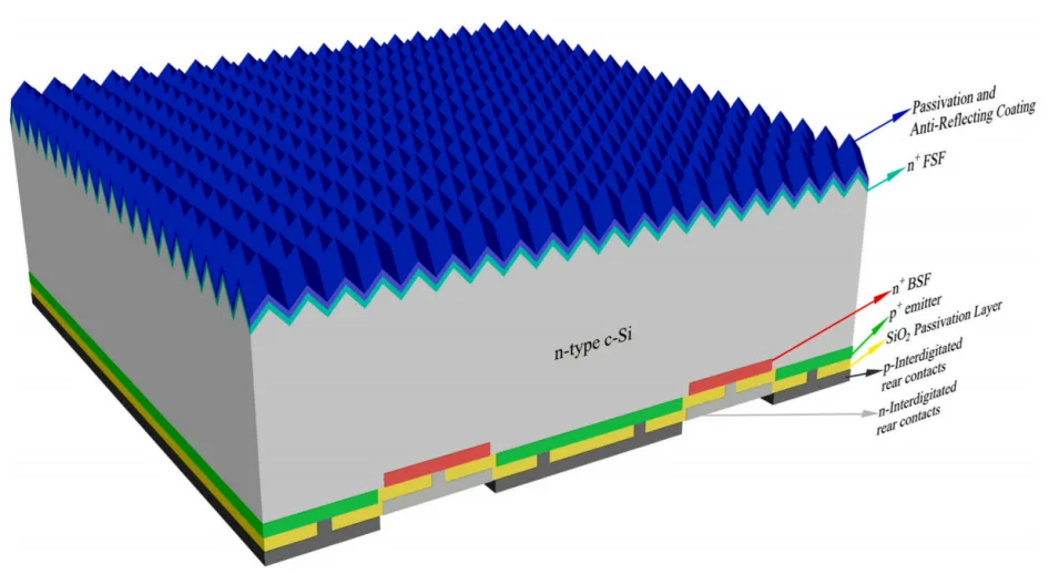
Cross-section schematic of the n-type IBC cell: rear interdigitated p+ emitter and n+ BSF contacts, front texturing and ARC.
The test cell has an area of 258.3 cm², wafer thickness of 151 ± 6 μm, a rear interdigitated period of about 480 μm, and emitter and BSF finger widths of roughly 250 μm and 90 μm. Illuminated measurements ran at AM1.5G, 100 mW/cm². At each temperature point, after thermal stabilization, five scans were averaged. The LeTID stress was measured directly at the stress temperature, without cooling down mid-test, and logged at exponential intervals of 1, 2, 4, 8 minutes and so on. Each parameter was normalized to its initial value, which separates the intrinsic degradation dynamics from the instantaneous temperature-coefficient effect.
Steady-State Thermal Sensitivity
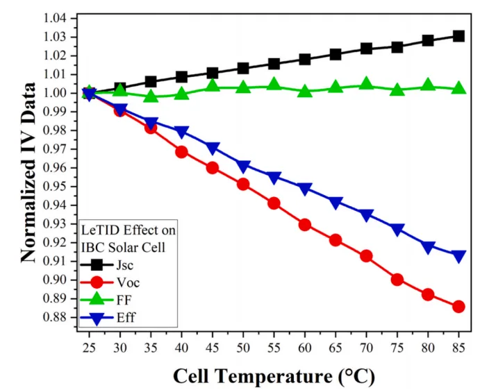
Normalized thermal evolution of four parameters relative to their own 25°C values.
At 25°C the cell shows Jsc around 38.6 mA/cm², Voc around 0.743 V, FF around 79%, and efficiency around 22.7%. Heating to 85°C, Jsc rises only about 3% (+0.0203 mA·cm⁻²·K⁻¹, roughly +0.05%/K). Voc falls linearly at −1.4 mV/K (about −0.2%/°C). Efficiency drops about 9%, and FF barely moves.
The small current increase comes from bandgap narrowing. Under the Varshni relation the absorption edge shifts toward longer wavelengths, so photogeneration gets a slight boost. The fast voltage decay comes from the exponential growth of J0(T), governed by intrinsic carrier concentration and recombination activity. Voc scales with ln(Jsc/J0), so a moderate rise in J0 is enough to cause a measurable loss.
This temperature coefficient sits in the −1.3 to −1.6 mV/K range common to high-quality crystalline silicon devices. It marks a recombination-limited cell rather than a resistance- or transport-limited one. After normalization the ranking is just as clear: at 85°C Voc drops about 15%, efficiency about 9%, FF stays within ±1%, and Jsc actually gains about 3%.
LeTID Dynamics
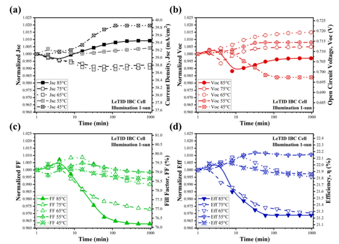
LeTID degradation dynamics.
Steady-state measurement only answers "how hot." The LeTID stress experiment fills in "how it changes over time." At 85°C, Voc drops fast in the first 10 to 30 minutes, then slowly approaches a quasi-saturation. At lower temperatures the decay is much gentler. After 960 minutes Voc falls to about 0.69 V, Jsc stays within ±2% throughout, FF wobbles slightly, and no regeneration shows up inside the experimental window. Since measurements were taken at the stress temperature after thermal stabilization, the early voltage drop should be attributed to rapid defect-state activation rather than transient thermal equilibrium. The stable Jsc says photogeneration and short-circuit extraction were not affected, so the dominant loss is not generation-limited. The authors also note a limitation: there is no dark-anneal control experiment, so the contribution of a pure thermal effect cannot be fully ruled out.
Dark-State Verification
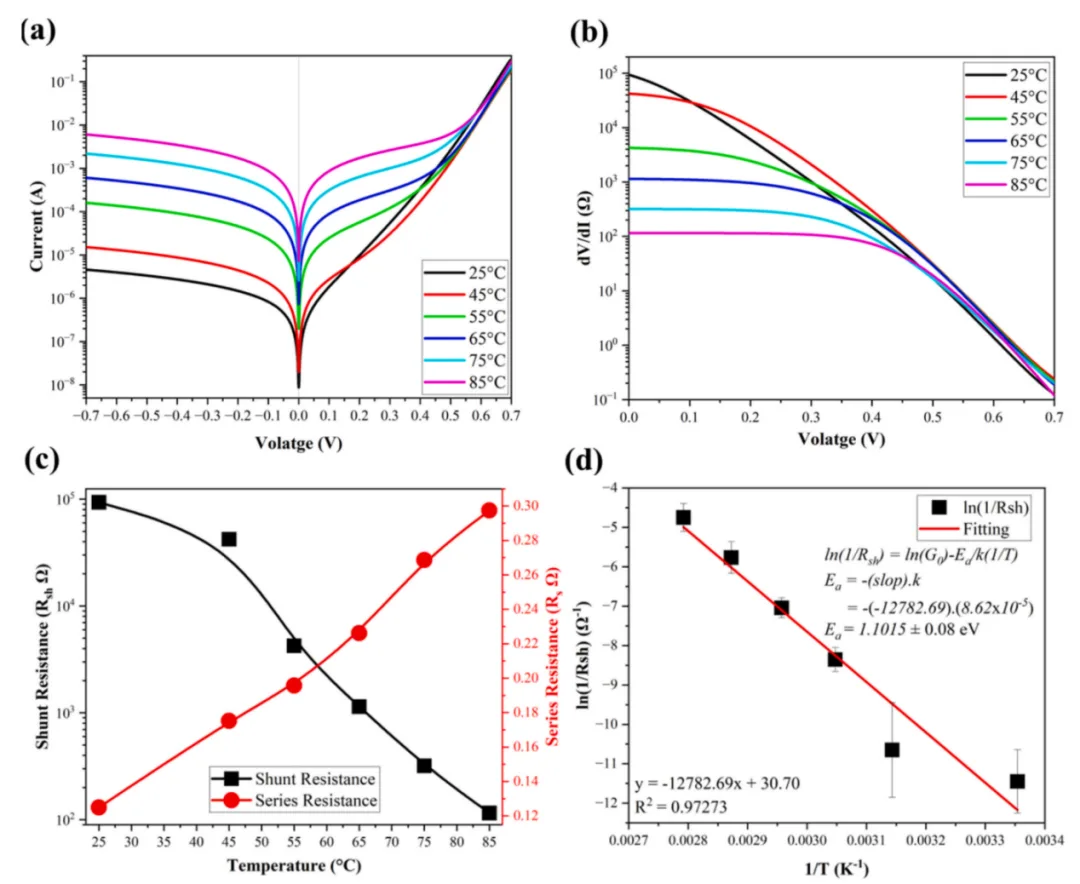
Dark electrical behavior and leakage channels: (a) dark J-V curves, (b) differential resistance, (c) extracted shunt and series resistance, (d) Arrhenius analysis of shunt conductance giving Ea ≈ 1.10 eV.
Dark I-V approaches the same problem from outside the illuminated regime. Forward current rises markedly with temperature. The low-bias slope shows shunt resistance dropping clearly, while the high-current region changes little. So the temperature-driven resistance evolution is dominated by leakage activation, not series-resistance degradation. The ideality factor holds at 1.05 to 1.25, meaning diffusion recombination dominates, with a possible SRH contribution at high temperature.
An Arrhenius analysis of the shunt conductance gives a good linear fit of ln(1/Rsh) against 1/T (R² = 0.97), with an activation energy of 1.10 ± 0.08 eV. That is comparable to the silicon bandgap (about 1.12 eV) and falls within the reported LeTID range of 0.8 to 1.2 eV. A bandgap-scale activation energy is often linked to deep-level defect-assisted conduction, but an intrinsic carrier concentration contribution cannot be excluded. So it supports thermally activated leakage behavior without pinning down a specific defect species.
Unified Framework and Field Extrapolation
Three lines of evidence converge into one phenomenological framework: J0(t, T) = J0,intr(T) + A·Ndef(t, T). On top of the intrinsic saturation current sits a thermally activated defect contribution that evolves with time and temperature. This then converts into voltage loss through Voc = (nkT/q)·ln(Jsc/(J0 + 1)). Recombination enhancement and leakage activation run in parallel inside the same expression. The steady-state temperature coefficient, LeTID dynamics, and dark leakage evolution are thereby tied together. The framework does not identify a specific defect identity.
Extrapolating to outdoor operation: under high irradiance, module cell temperatures often sit at 50 to 65°C. Using −1.4 mV/K, 60°C relative to 25°C means about 49 mV of voltage loss, and temperature-accelerated LeTID adds time-dependent loss on top of that. The conclusions apply only to the measured cell. For back-contact TOPCon and back-contact HJT they are only a qualitative reference: degradation magnitude, activation energy, and regeneration dynamics depend on each one's passivating-contact scheme, interface quality, hydrogen distribution, and thermal stability, and deserve dedicated comparative study. For high-efficiency back-contact devices in warm climates, voltage robustness and long-term energy yield ultimately rest on rear passivation stability and defect management.
Ooitech's View
What strikes us here is how much of that 49 mV outdoor loss lives on the rear side, where passivation and contact quality make or break long-term Voc. On the module line the story is the same: how you cut, string, and laminate an IBC cell decides whether that rear stability survives into the field. Having built turnkey lines for IBC and HPBC layouts, we see LeTID robustness as a process-and-materials problem as much as a cell one. Worth a follow on our YouTube channel www.youtube.com/ooitech if you want to see how back-contact modules actually get built.