Pinholes in TOPCon Cells: The Surprising Path
Table of Contents
Quick answer: Research on TOPCon cells has found that deliberately leaving a controlled amount of thin oxide can improve passivation rather than degrade it, which reverses a long-held assumption. The study measured oxide layers in the range of 0.2 nm and 0.3 nm against a reference at 1.7 nm, and found that the thinner, deliberately retained oxide did not simply add resistance. The tunnel oxide in a TOPCon cell has to be thin enough for carriers to tunnel through and thick enough to passivate the surface, and the conventional target sits at one or two nanometres. What the result suggests is that the boundary is less sharp than assumed, and that the chemical state of the interface matters as much as the thickness. For a production line, that shifts attention toward interface control rather than thickness alone.
PV Module Manufacturing · by Jerry, Ooitech
Overview
Here is something that flips a long-held assumption in silicon PV. Researchers found that deliberately leaving certain "pinholes" in the SiOx layer of a TOPCon cell can push efficiency up to 26.55%, instead of dragging it down.
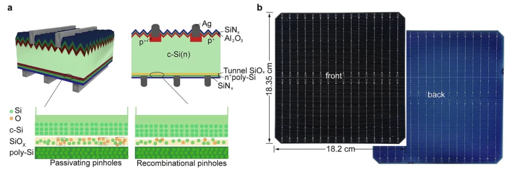
The key finding: pinholes in the tunnel oxide split into two families. One is the recombination type (oxygen-depleted, where poly-Si contacts c-Si directly, bad), the other is the passivating type (residual oxygen stays behind, passivating dangling bonds while still allowing tunneling, good). The passivating type measures about 1.6 ± 0.2 nm × 1.4 ± 0.3 nm in cross-section, with an areal density of 2 × 10¹² cm⁻². A Fischer model showed that what decides device performance is not pinhole geometry, but whether the pinhole is passivated.
Reference: Passivating pinholes for large-area and high-efficiency silicon solar cells with tunnel oxide passivated contact, Nat Commun 17, 2490 (2026). https://doi.org/10.1038/s41467-026-70511-2
Research Background and the Problem That Stuck
TOPCon is now the mainstream for n-type silicon. Runergy hit 26.55% on 335 cm², Jinko stacked TOPCon plus perovskite to 33.24%, and single-side n-TOPCon has a theoretical ceiling of 27.79%. But nobody had pinned down what role the pinholes in that interfacial SiOx layer actually play.
The traditional view: pinhole means poly-Si pokes straight into c-Si, oxygen passivation fails, bad news.
The reality is messier. Oxide too thick (>1.7 nm) passivates well but tunnels poorly, so FF collapses. Oxide too thin (<1.3 nm) means more pinholes, and now you worry about Voc collapsing.
The authors broke oxide thickness plus oxygen distribution into three cases (the Introduction section):
Case 1: thick oxide, passivation OK, tunneling not optimal
Case 2: thin oxide plus oxygen depletion, giving recombination-type pinholes (the classic "bad pinhole")
Case 3: thin oxide but oxygen still seeps into the pinhole, giving passivating-type pinholes (the new finding here)
Before this, HR-TEM resolution wasn't good enough to see features below 2 nm. Literature reported pinhole diameters of 5 nm to 200 nm and densities of 10⁶ to 10⁸ cm⁻², which were all just "big holes". Selective etching and c-AFM rely on the etch rate difference between Si and SiOx, so regions with residual oxygen simply don't etch open. Passivating pinholes were naturally screened out by these methods. That's why Case 3 went unseen for so long.
Mechanism: Two Types of Pinhole (Figure 2)
Aberration-corrected HAADF-STEM (JEM ARM200F plus Spectra 300, 200/300 kV) scanned the poly-Si/SiOx/c-Si interface on a high-efficiency wafer (25.40%) and a low-efficiency control (24.07%).
| Type | Oxygen state | Size (high/low efficiency) | EELS O-K edge |
|---|---|---|---|
| Recombination | Oxygen-depleted, poly/c-Si lattice directly joined | Low-efficiency wafer ~1.37 × 1.35 nm | Deep oxygen valley |
| Passivating | Residual oxygen present, dangling bonds passivated | High-efficiency wafer 1.55 × 1.25 nm | Oxygen signal still visible, shallow oxygen valley |
Key point: the pinholes on the high-efficiency wafer are actually smaller, and retain oxygen better. All sizes are an order of magnitude smaller than earlier literature reported.
The Fischer point-contact model results (Fig. 3d in the original):
Pinhole area fraction f = πr²/P², but J₀ is insensitive to f. What really dominates is the surface recombination velocity S at the pinhole.
Around f ≈ 0.1, once S ≳ 10³ cm/s, J₀ climbs steeply, and it saturates above S > 10⁵ cm/s.
Meaning: the key to high performance isn't "zero pinholes", it's "pinholes that are passivated". This is the biggest highlight of the whole paper.
On density, this is a bit of a revolution. Statistics from X-Y orthogonal slicing across 40 wafers (high plus low efficiency) gave 2 × 10¹² cm⁻² for passivating and 3 × 10¹² cm⁻² for recombination pinholes, 4 to 6 orders of magnitude higher than literature values.
Three reasons stack up: first, the concept changed, so previously screened-out passivating nanodefects became visible; second, the samples are industrially optimized wafers above 25%, not test structures; third, the method is atomic-level HAADF, and indirect approaches simply can't see the sub-2 nm oxygen-containing region. To guard against overlap along the beam direction from 50 to 150 nm thick TEM samples, the authors backstopped with 4D-STEM ptychography along the thickness direction, confirming the density statistics aren't distorted by projection overlap.
Process Landing Point: Two-Step Oxidation plus Back Polishing plus Poly Triple Coupling
The variables from the original Methods plus SI (Supplementary Table 1):
Two-step oxidation: first O₂ oxidation into thin SiO₂, then an oxygen-starved step (no oxygen fed in). The passivating type needs longer oxygen flow time, higher temperature, larger flow, and higher pressure, which favors uniform, dense oxide.
POCl₃ diffusion: lower deposition temperature plus shorter time improves poly crystallization and suppresses recombination-type pinholes.
Back polishing morphology sits upstream of oxide thickness uniformity. All three have to be tuned together to stably produce Case 3.
Performance Comparison (Fig. 4 Hard Data)
Symmetric double-side poly-Si/SiOx samples (n-Si 1–3 Ω·cm, double-side polished):
τeff: 8.9 ms high efficiency vs 2.96 ms control (injection 5×10¹⁵ cm⁻³)
J₀: 2.6 vs 10.6 fA/cm²
ΔVoc measured at 15.9 mV, but the J₀ difference alone explains only ~11 mV. The remaining ~5 mV the authors attribute to improved bulk SRH lifetime. The optimized anneal, while creating passivating pinholes, also getters metal impurities (citing Krügener's 25% POLO work). Fixing both interface and bulk together is the recipe for crossing 25%.
For FF, the difference mainly comes from Rs:
Rs: 357 (high efficiency) vs 619 mΩ·cm² (control), Suns-Voc measured
ρc (TLM): 4.6 vs 5.4 mΩ·cm²
The counterintuitive point: by "denser pinholes lower ρc" logic, more passivating pinholes on the high-efficiency wafer should mean lower ρc, and indeed 4.6 < 5.4. But the authors add a twist. Near recombination-type pinholes, phosphorus diffuses into the wafer, while passivating types are blocked by oxygen (the EDS doping profile in Supplementary Fig. 10). So doping profile and contact resistance follow two separate logics, and you can't explain them by pinhole density alone.
PL was uniform across the full wafer, and Corescan mapping of Voc distribution also held up for large-area uniformity.
One Line for the Industry
This paper pushes the TOPCon interface from a binary story of "intact oxide vs pinhole leakage" to a ternary one: "pinholes can be good too, as long as oxygen is still there". What the industry needs to do next isn't to obsess over zero pinholes, but to tune the back polishing to oxidation to poly deposition chain so that pinholes carry oxygen. Daheng's wafer at 25.40% on 333.3 cm² has already proven the road works.
Ooitech's View
What strikes us here is how much of this hinges on the process chain, not just the cell design. That two-step oxidation, POCl₃ tuning, and back polishing all have to move together is exactly the kind of coupling that gets lost when a line is assembled piecemeal. On the module side we see the same pattern, where lamination and stringing tolerances quietly decide whether a good cell keeps its Voc. If you want a closer look at how these interface-sensitive processes translate onto a real production floor, our factory walkthroughs on YouTube (www.youtube.com/ooitech) are worth a subscribe.