Perovskite/Silicon Tandem Cells: 8nm ITO Interconnect
Table of Contents
Quick answer: Monolithic perovskite/silicon tandem cells stack a perovskite top junction directly on a silicon bottom junction, with a thin transparent interconnect layer between them. That interconnect is the engineering crux: it has to pass current from one junction to the other, stay optically transparent across the wavelengths the bottom cell needs, and survive the processing of the layers above. In this work the interconnect is an indium tin oxide layer about 8 nm thick, sitting within a stack that includes layers at 15 nm, 30 nm, 110 nm and a 600 nm region, with a 10 µm feature elsewhere in the device. The measurements used span visible wavelengths from the blue end through to the near-infrared. Because the layer is only a few nanometres, its continuity and doping matter as much as its thickness.
PV Module Manufacturing · by Jerry, Ooitech
Product Introduction
Monolithic perovskite/silicon tandem solar cells are one of the clearest routes past the efficiency ceiling of single-junction devices. The top cell and bottom cell are connected in series through a recombination interconnect layer, and how good that interface is decides whether carriers can be transported and recombined smoothly. The trouble sits on the micro-pyramid textured surface of the silicon heterojunction (SHJ) bottom cell. The pyramids run about 600 nm tall, and on that terrain the recombination layer suffers optical parasitic loss while the self-assembled monolayer (SAM) never spreads evenly. Over time this drags device performance down.
This work measured indium tin oxide (ITO) interconnect layers from 2 to 30 nm thick and found that an ultrathin 8 nm layer works best on two fronts at once: cutting optical loss and improving surface potential uniformity. Once NiOx modification and Poly-SAM functionalization were stacked on top, the short-circuit current density rose by 0.85 mA cm⁻² to reach 20.82 mA cm⁻², the power conversion efficiency hit 31.80%, and after 500 hours of maximum power point tracking the device still held 96% of its initial efficiency.
Experimental Method
The SHJ bottom cell used n-type silicon wafers, 110 ± 10 µm thick, KOH double-side textured into pyramids about 600 nm tall. After RCA cleaning, PECVD deposited passivation and doped layers in sequence: the front side got 8 nm intrinsic a-Si:H(i) plus 15 nm n-type nc-SiOx:H(n), the back side got 8 nm p-type a-Si:H(p), then 110 nm ITO was sputtered and 700 nm Ag evaporated on the back. On the front, six ITO interconnect thicknesses were deposited separately: 2, 5, 8, 10, 20 and 30 nm, annealed at 180°C and laser scribed.
The perovskite top cell followed this route. The bottom cell was annealed and UV-ozone treated first, then NiOx was deposited by magnetron sputtering, followed by another anneal and UV-ozone step. Inside a nitrogen glovebox, Poly-SAM was spin-coated (0.5 mg mL⁻¹, solvent methanol and chlorobenzene at 1:1) and annealed at 100°C. The perovskite was Cs₀.₀₅FA₀.₈MA₀.₁₅Pb(I₀.₇₅₅Br₀.₂₅₅)₃ with a 1.68 eV bandgap, spin-coated in two steps, with chlorobenzene dripped as antisolvent during the high-speed stage and baked at 100°C for 20 minutes. The surface was tweaked with PDADI, then C₆₀ was thermally evaporated, SnO₂ grown by ALD, 45 nm IZO sputtered, Ag electrodes evaporated, and finally an MgF₂ anti-reflection film capped the stack.
Technical Advantages
ITO Interconnect Layer Optoelectronic Properties
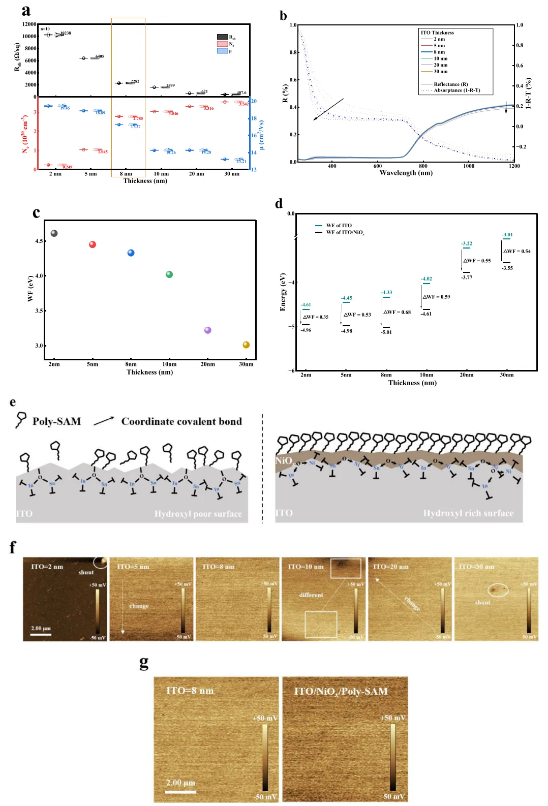
(a) Rsh, Ne and µ versus thickness (n = 10); (b) optical absorptance and reflectance of the ITO layer; (c) work function versus thickness; (d) work function shift (ΔWF) before and after NiOx treatment at different thicknesses; (e) schematic of SAM distribution on NiOx-modified ITO; (f) KPFM surface potential maps of 2–30 nm interconnect ITO; (g) KPFM surface potential maps of 8 nm interconnect ITO before and after NiOx and Poly-SAM functionalization.
Hall effect measurements showed sheet resistance dropping as film thickness increased, which is what you would expect. Carrier concentration stayed fairly steady between 8 and 30 nm, around 2.8 to 3.5 × 10²⁰ cm⁻³, but once you go below 8 nm it starts to fall off. Mobility dipped only slightly across the narrow 2 to 8 nm window, a sign the film integrity was still intact. 8 nm lands right in the sweet spot where sheet resistance is low enough and the electrical performance has not collapsed.
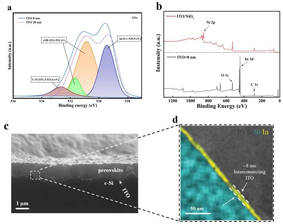
(a) Peak-fitted O 1s high-resolution XPS spectrum of the ITO layer on the textured c-Si bottom cell surface. (b) High-resolution XPS spectra of the 8 nm ITO layer on the textured c-Si bottom cell before and after NiOx modification. (c) Cross-sectional SEM image of the 8 nm ITO layer on the textured c-Si bottom cell. (d) Corresponding EDS elemental maps of the focused region of the 8 nm ITO sample, with the color-element legend in the top right.
Optically, thinning the ITO pulled both reflectance and absorptance down above 450 nm, thanks to destructive interference plus weaker free-carrier absorption.
UPS showed the work function rising as thickness shrank, and after NiOx modification and annealing the work function shift peaked at 8 nm.
KPFM area scans revealed that sub-10 nm ITO suppressed all the local shunt points, with 8 nm giving the best uniformity.
XPS turned up an interesting detail: the 8 nm ITO surface had a higher hydroxyl density than the 20 nm one, and those hydroxyls formed In─O─Ni bridge bonds with NiOx, letting the NiOx spread more evenly and adhere more firmly. After modification the In signal vanished entirely, which says the coverage layer quality was excellent and laid a good foundation for the SAM self-assembly that follows.
SEM and EDS also confirmed the 8 nm ITO gave conformal coverage over the texture.
Tandem Cell Photovoltaic Performance
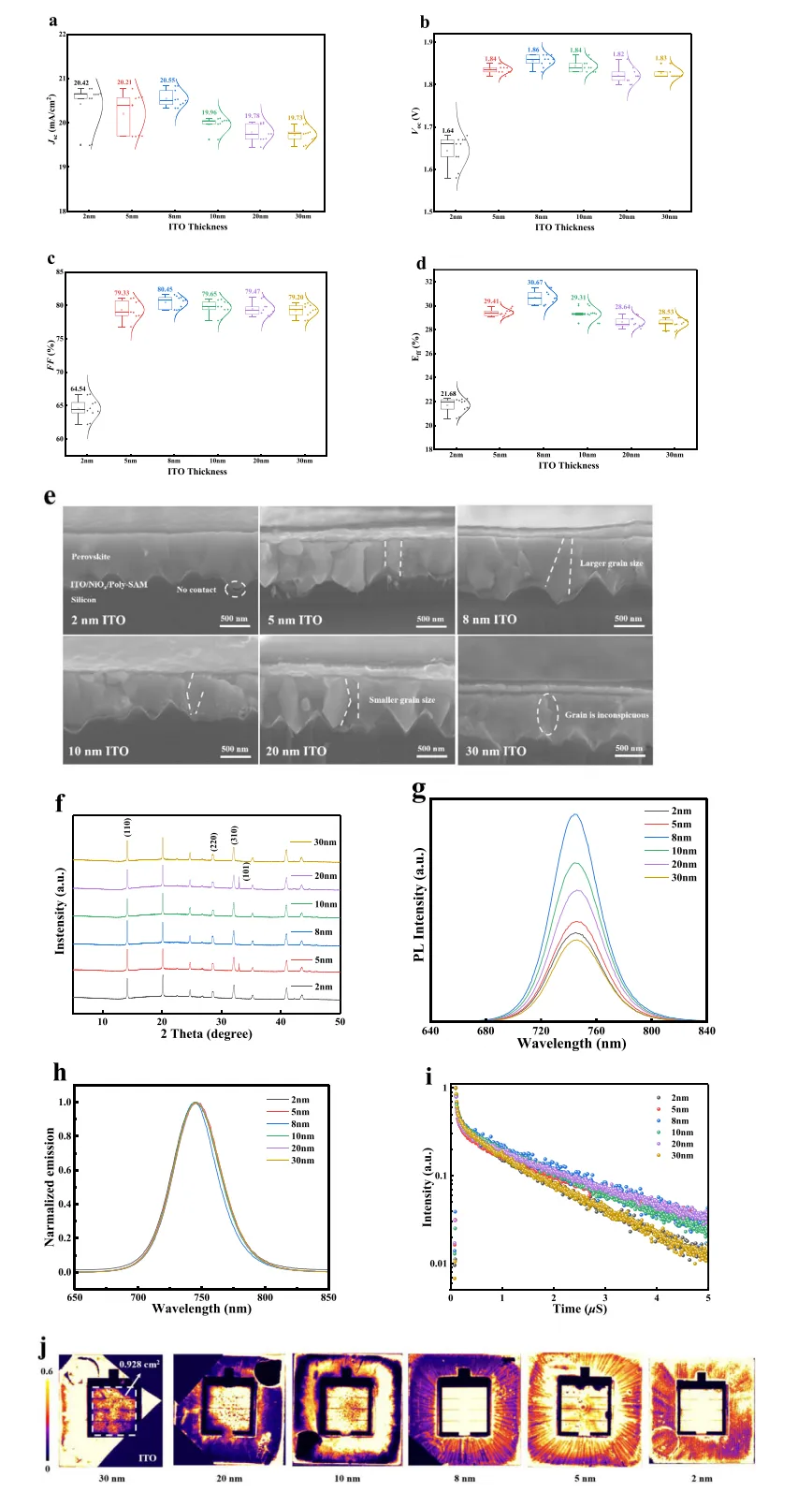
(a) Variation of Jsc in perovskite/silicon tandem cells; (b) variation of Voc; (c) variation of FF; (d) variation of PCE; (e) cross-sectional SEM image of the tandem cell on ITO; (f) XRD pattern of the perovskite film on ITO; (g) steady-state PL spectrum of the perovskite film on ITO; (h) normalized steady-state PL curves; (i) transient TRPL decay spectra of the perovskite film on ITO; (j) photoluminescence image of the tandem cell, active area 0.928 cm².
All six ITO interconnect thicknesses went through J-V testing.
Below 5 nm, Voc and FF dropped hard. Voc could not be pushed past 1.7 V and PCE came in at just 21.68%, mainly because the film was already discontinuous on the pyramid texture.
8 nm was the best answer. Cross-sectional SEM showed perovskite grains larger and denser on the ultrathin ITO (under 10 nm), and XRD confirmed better crystalline quality, though the 5 nm sample threw up a PbI₂ peak, a sign degradation had already begun. Steady-state PL intensity climbed all the way from 30 nm down to 8 nm, then fell again, so 8 nm sat right at the peak, matching the lowest defect density.
The normalized PL characteristic peak did not shift, meaning the nature of interface non-radiative recombination stayed the same. TRPL carrier lifetimes were likewise longest at 8 nm. These results trace back to the stronger net dipole and more uniform work function that Poly-SAM brings, lifting Voc and FF together. PL imaging also exposed sub-micron non-uniformity inside the perovskite sub-cell, but the ultrathin high-resistance ITO layer has high lateral resistivity, so the reach of local shunting was effectively boxed in and never dragged the whole device down.
Current Density Improvement
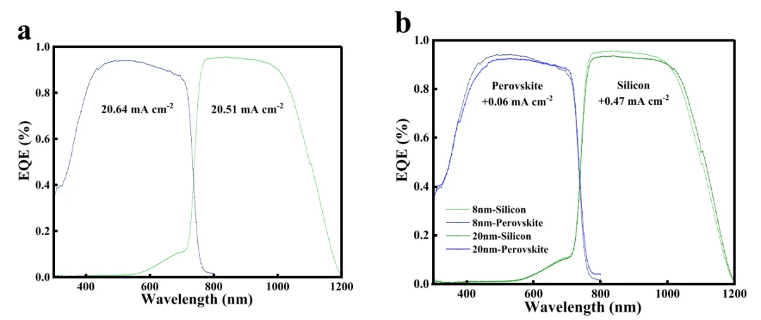
(a) EQE curves of the perovskite and silicon sub-cells under the 8 nm ITO interconnect layer; (b) EQE curves of the initial and optimized tandem cells.
The front IZO layer was rated by the figure of merit Aw × Rsheet⁻¹, and 45 nm came out best. Thinning the interconnect ITO from 20 nm to 10 nm to 8 nm pushed the average Jsc from 19.78 to 19.96 to 20.55 mA cm⁻². The EQE-integrated current densities of the perovskite and silicon sub-cells were 20.64 and 20.51 mA cm⁻² respectively, in line with the J-V data. Against 20 nm ITO, 8 nm handed the perovskite sub-cell an extra 0.06 mA cm⁻² and the silicon sub-cell an extra 0.47, with the near-infrared contribution from the silicon bottom cell gaining the most.
Product Application
Device Performance and Stability
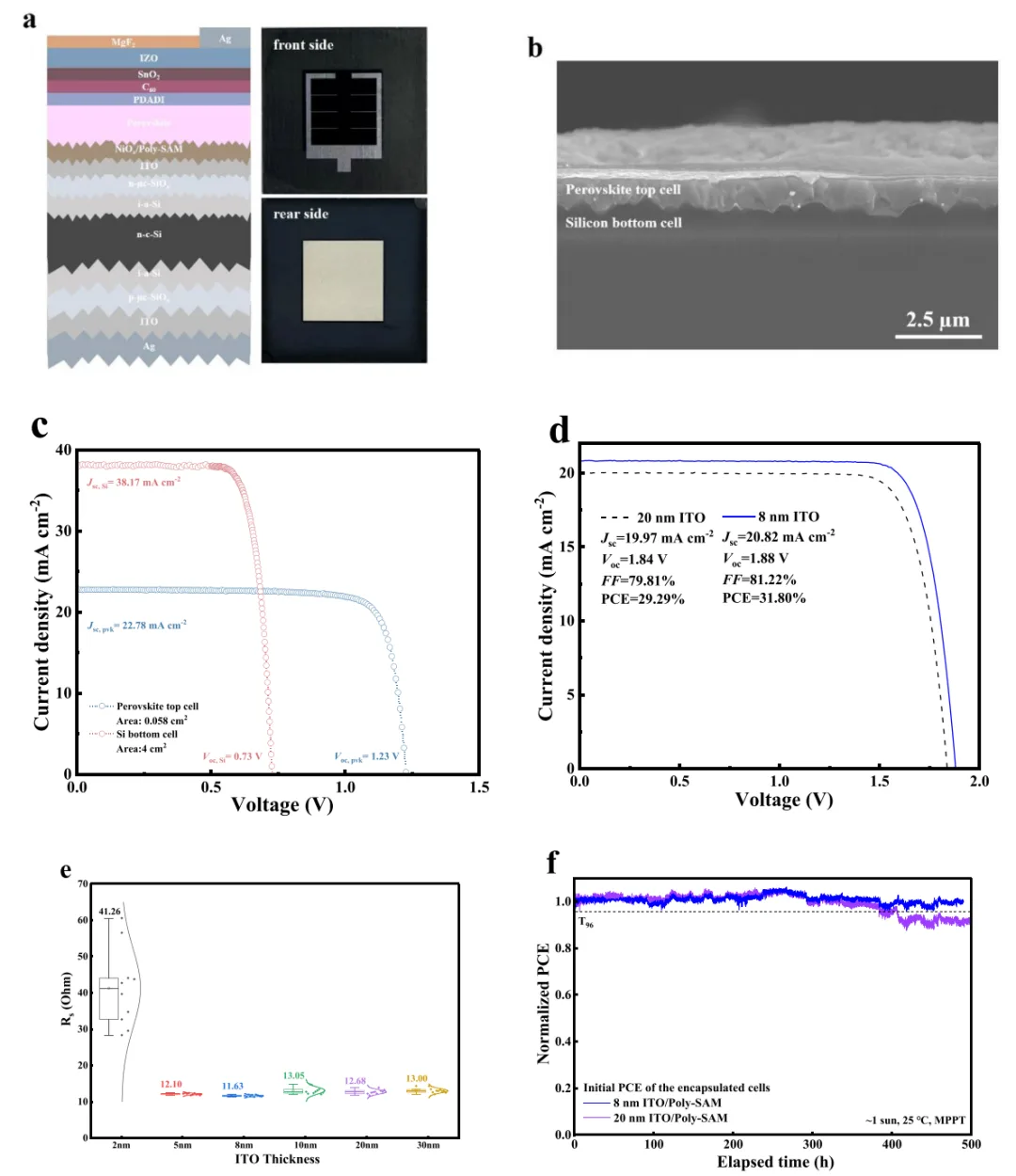
(a) Schematic structure and photograph of the perovskite/silicon tandem solar cell; (b) cross-sectional SEM image of the tandem cell; (c) J-V curves of the single-junction perovskite and silicon sub-cells; (d) representative J-V curve of the high-performance cell; (e) variation of Rs in perovskite/silicon tandem cells built on 30 nm to 2 nm ITO interconnect layers; (f) MPPT test results of the encapsulated tandem cell under 1-sun illumination.
Once the ITO interconnect thickness was dialed in, the average PCE of the tandem devices rose from 28.64% to 30.67%. The 2 nm ITO carried a series resistance Rs as high as 41.26 Ω, so the series connection was essentially broken. The 8 nm Rs was far lower, internal impedance came down, and the voltage loss near the maximum power point shrank. On stability, the 8 nm ITO tandem cell held 96% of its initial PCE after 500 hours of MPPT, while the 20 nm one kept only 90%, putting it among the most stable in the TCO/SAM interconnect family. Why so stable? Poly-SAM coverage is high, and the perovskite crystallization improves along with it.
Regions covered by SAM have low surface energy, and the phosphonic acid groups coordinate with Pb²⁺ and FA⁺, guiding the perovskite to grow slowly and in an ordered way, so the grains come out big. On bare ITO regions there is no such template effect, nucleation runs fast and disordered, and grains end up small with plenty of grain boundaries. On top of that, Poly-SAM passivates the unsaturated bonds and halide vacancies at the interface, halide migration gets suppressed, and degradation slows. The uniform surface potential that ultrathin ITO itself brings helps too, and with several factors stacking together the device lifetime goes up.
The MPPT stability testing here relies on an LED solar simulator of 3A+ grade as the aging light source, which can control cell temperature and the surrounding atmosphere in several ways to run long-term stability testing.
Conclusion and Outlook
8 nm is the optimal ITO interconnect thickness for perovskite/silicon tandem cells. This thickness both lifts perovskite crystalline quality and holds down parasitic absorption. After NiOx modification and Poly-SAM functionalization, the surface potential grows more uniform and the work function shift more pronounced. The 8 nm ITO surface carries more hydroxyls, NiOx spreads evenly, the SAM packs densely, and the conformal coverage over the texture was verified by SEM and EDS. Against the conventional 20 nm ITO, the optimized device reached a champion efficiency of 31.80%, with Jsc up by 0.85 mA cm⁻² and 96% of initial efficiency retained after 500 hours of MPPT.
Looking ahead, there is still plenty to improve. The rear texture and optical reflector can be refined further to strengthen the light trap in the silicon bottom cell, raise its current, and nail the current matching. FF and Voc remain the bottlenecks limiting overall efficiency, so contact passivation strategies need to go deeper. Alternative interconnect architectures like silicon-based tunnel junctions are worth trying too. When it comes to scaling up to production, TCO thickness and metallization grid design have to be tuned together, so that over large areas the shading is not too heavy and the lateral conduction does not suffer. And with a thinner layer, indium usage drops, so sustainability benefits as well.
Ooitech's View
What stands out here is that a few nanometers of ITO can swing both optics and crystallization on that 600 nm pyramid texture, and that same conformal-coverage problem is exactly what shows up when tandem lines move from lab coupons to full-size modules. On the production floor the tabber-stringer, layup and lamination steps all have to respect these fragile interconnect and SAM interfaces, which is where uniform, well-tuned module-line equipment earns its keep. If you want to see how these processes look at real factory scale, the Ooitech YouTube channel at www.youtube.com/ooitech is worth a follow.
Related: Perovskite in space: what 100 thermal shock cycles cost looks at the same absorber family through interconnect design rather than through thermal shock.
Further reading and background data
Public reference material on this topic, published by the organisations that maintain the industry's technology roadmap and market data: