The Evolution History of Photovoltaic Wafer Sizes
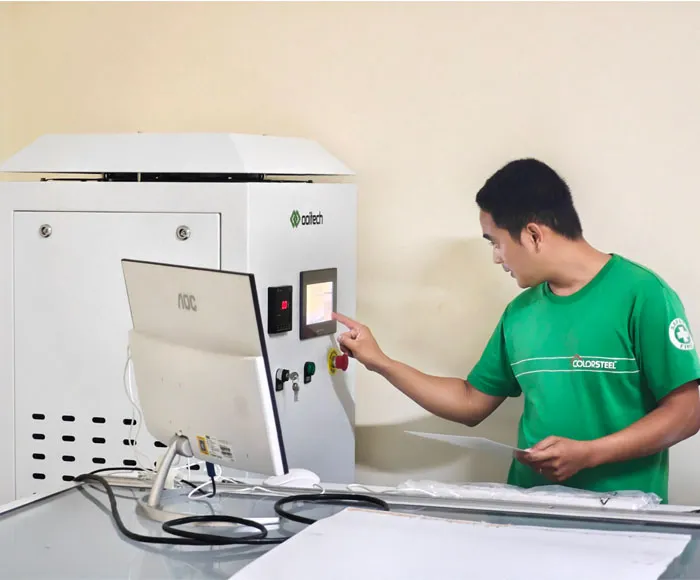
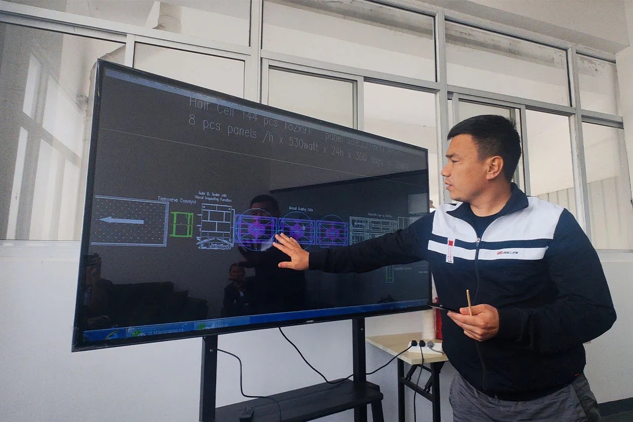
Product Introduction
If you have followed the development of photovoltaic wafers, you will know that the edge length of solar wafers has grown from 100mm to 125mm, then to 156mm, and all the way up to today's 210mm.
We can clearly see that as the photovoltaic industry has matured, wafer sizes keep getting larger. So what kind of impact does a larger wafer size bring to the entire PV industry chain? And what are these size changes actually based on?

Impact on the PV Industry Chain
1) Wafer Manufacturers
Larger wafer sizes help wafer companies reduce three major costs: silicon material, crystal pulling, and slicing.
The core equipment for wafer manufacturing (such as single-crystal furnaces and slicing machines) is usually measured by "batches per hour" or "slices per machine shift". A larger size means a single furnace or single machine produces more wafers per run. For example, the area of a 210mm wafer is about 1.82 times that of a 156mm one, so if the slicing yield stays the same, the hourly output of a single slicing machine can increase by more than 80%.
Fixed costs such as equipment depreciation, energy consumption, and labor get spread across a larger wafer area, so the non-silicon cost per wafer (like electricity and materials) drops noticeably. According to industry data, upgrading from 156mm to 210mm can lower the non-silicon cost of the wafer stage by roughly 20%-30%.
2) Cell Manufacturers
Larger wafers reduce the "edge loss" of cells, since the bigger the wafer area, the lower the proportion of invalid edge regions.
The "line speed" of cell production is basically fixed (such as the cycle time of PECVD and screen printing), so a larger size increases the cell output of a single production line proportionally, and lowers the consumable cost of silver paste, targets, and other materials per cell. For example, the silver paste consumption of a 210mm cell is about 1.3 times that of a 182mm cell, but the area is 1.82 times larger, so the silver paste cost per watt actually drops by about 28%.

3) Module Manufacturers
Cells made from larger wafers force the module size to grow, which lets module manufacturers reduce packaging costs and achieve higher power density.
The core costs of module packaging are auxiliary materials such as glass, encapsulant film, frames, and junction boxes, along with the labor and equipment costs of processes like stringing and lamination. A larger size means less auxiliary material is used per watt, and the labor cost per watt is also reduced.
4) Power Plant Investors
Larger modules can deliver higher power density (for example, 210R cell modules have reached 600W+, and 700W+ modules made from 210 cells are already in mass production), reducing the number of modules, the amount of mounting structures, and cable length a plant requires, which indirectly lowers the cost for power plant investors.

The continuous growth of wafer sizes is essentially a collaborative upgrade of "cost reduction and efficiency improvement" for wafer manufacturers, cell testing, module manufacturers, power plant investors, and many other parties. By scaling up the production unit size and lowering the unit cost, the dividends are passed down the chain to the downstream players.
Technical Parameters
| Wafer Size | Crystal Platform | Area Increase | Typical Module Power | Notes |
|---|---|---|---|---|
| 125mm (5 inch) | 6 inch | Baseline | - | Phased out after 2012 |
| 156mm (6 inch) | 8 inch | Baseline | - | Mainstream for years |
| M1 (156.75-φ205mm) | 8 inch | +2.2% | +5W vs prior | Released end of 2013 |
| M2 (156.75-φ210mm) | 8 inch | +2.2% | +5W vs prior | Became mainstream |
| 158.75mm | 8 inch | Minor | - | Low retrofit cost |
| 166.00mm | 8 inch | +12.22% vs M2 | 420-430W (72-cell) | Near equipment limit |
| M10 (182mm) | New platform | - | 500W+ | Released June 2020 |
| G12 (210mm) | New platform | - | 600W+ | Released August 2019 |
| 210*182.2mm (Rectangular) | New platform | - | Golden size module | Released 2023 |
Technical Advantages
Larger wafers lower silicon material, crystal pulling, and slicing costs at the manufacturing stage
A single slicing machine can increase hourly output by more than 80% when moving from 156mm to 210mm
Non-silicon cost of the wafer stage can drop by roughly 20%-30% when upgrading from 156mm to 210mm
Reduced edge loss and lower silver paste cost per watt (about 28% lower for 210mm cells)
Higher power density modules cut the number of modules, mounting structures, and cable length needed
Product Application
The History of PV Wafer Development
Since photovoltaic wafers originally came from semiconductor single-crystal materials, the PV industry has long followed the semiconductor wafer sizes of 6 inch and 8 inch (diameter), corresponding to the so-called 5-inch wafer (125mm) and 6-inch wafer (156mm) in terms of edge length.
As the PV industry grew and demand for wafers and cells increased, and with the progress of domestic crystal pulling, slicing, and cell production equipment, the 5-inch wafer (125mm) gradually exited the PV chain. After 2012, except for one or two special cell manufacturers, the 125mm wafer was basically phased out by the market.
156mm (8-inch crystal growth) wafers then became the mainstream size. After that, the industry began experimenting with small increases on the 8-inch crystal growth platform. At the end of 2013, five companies including Zhonghuan and Longi jointly released the M1 (156.75-φ205mm) and M2 (156.75-φ210mm) wafer standards. Without changing the module size, M2 raised the wafer area (by 2.2%) and boosted module power by more than 5W, quickly becoming the industry mainstream and staying stable for several years.
In the following years, major wafer manufacturers used technical upgrades on the basis of M1 and M2 to keep raising the wafer edge length to 158.75, 161.7, 166mm and other sizes. The advantage of the 158.75mm wafer is that all existing internal capacity could be upgraded through technical retrofitting at low cost. Even for very old cell plants, the 1GW retrofit cost stayed within an acceptable range.
The advantage of the 166.00mm wafer is that its area is 12.22% larger than M2, and modules of the 72-type using this wafer could reach 420-430W. At the same time, this size was close to but did not exceed the capacity limit of existing equipment, so the retrofit cost remained controllable.
From 156mm to 166mm, all manufacturers in this stage were increasing the wafer area through technical upgrades on the existing 8-inch crystal growth platform.

In August 2019, Zhonghuan made a leap and released the G12 single-crystal wafer with a 210mm edge length, directly applying the semiconductor wafer size specification to PV. The goal was to achieve a leap in module power and a further reduction in manufacturing cost through larger wafers. But at that time, the 210 wafer had almost no upstream or downstream industry support in the PV chain, and most of the industry was skeptical about 210.
In 2019, Trina and Zhonghuan, the earliest adopters of the 210 wafer, released the next generation of new module products. Based on the 50-version of the 210 wafer, the maximum power reached 500W, which was also the first 500W product in the PV industry. Limited by the PV glass specifications of the time, the module could not be made into 6 columns of cells and could only be made into an odd number of 5 columns, and the odd column layout meant the module had to use a fly-wire design. Also limited by the inverter current at the time, the cells could not use the half-cut that was mainstream in the industry, and could only be made into thirds.

With the release of Zhonghuan's 210 edge length wafer and the advantage that 210 modules could reach 500W+ power, by the end of 2019, module leaders represented by Jinko, JA Solar, and Longi fell into deep thought. On one hand, these companies wanted a product to counter the impact of the 500W module; on the other hand, they did not want to make products with odd columns and thirds-cut designs.
So these three companies did not choose 210, and they all coincidentally thought of using the traditional even-numbered 6-column cell layout to achieve 500W+ products. In fact, the specifications of the three were not the same at first. Jinko and JA Solar roughly settled on a 180mm wafer size at the end of the first quarter of 2020, while Longi initially determined a size of 17X. After communication and negotiation, the three companies finally unified the size to 182mm, and in June 2020, the three leading companies, together with 7 other manufacturers in the industry, jointly released the M10 single-crystal wafer based on the 182mm specification.
The 183.75*182.2 cell size used today is based on the 182mm technical foundation. Just like the previous 156mm edge length kept increasing to 158.75, it raises the cell area through technical upgrades without changing the module size, improving power generation efficiency.

The logic of the 182 edge length wafer is different from the leapfrog introduction of the 210 edge length. 182 was generated through a reverse-deduction logic based on the industry's existing boundary conditions. The main boundary conditions were the height of the shipping container and the width of the glass furnace. These two points determined that the upper limit of the module width is between 1133-1134mm, which then leads to a cell size of 182mm for a 6-column cell layout.

On one hand, the power of the 182 module is higher than the previous 50-version 210 module. More importantly, the 182 module fully continued the mature 6-column layout and 2-cut cell technical solution, with better product performance and a mature supporting upstream and downstream supply chain. By the industry's thinking logic at the time, 210 could not be made into a 6-column cell layout, both because the glass furnace did not support it and the container did not support it. It seemed that 210 was about to become a failed solution.

However, Trina, the leader of the 210 camp, broke through the fixed thinking of most industry practitioners and subverted the traditional design logic, quickly launching a 60-cell 210 module product based on a 6-column cell layout and 2-cut cells, with a module power reaching up to 600W (the module with a size of 2172*1303).
Trina's idea was: if the container does not support two-layer side placement of 6-column 210 modules, then simply place the modules vertically in the container; if the glass furnace does not support it, then join hands with glass factories to upgrade the production line; if the 2-cut 210 cell current is too high for the inverter, then cooperate with inverter manufacturers to develop a new generation of products. In the second half of 2020, Trina also led a group of manufacturers to establish the 600W+ industry alliance, aiming to achieve coordinated promotion of the entire 210 industry chain.

The 6-string version of the 210 module reached a width of 1303mm and could only be placed vertically in the container. Vertical placement caused certain problems in some scenarios, and many customers did not like this method. Facing this problem, in mid-2022, Trina boldly proposed the rectangular wafer solution, launching a 182mm210mm rectangular wafer. The module based on the rectangular wafer has a width of 1134mm, consistent with the traditional 182 module width, while the length is 238X. Then in 2023, 9 leading enterprises including Jinko, JA Solar, and Longi jointly released the size of the rectangular wafer module, confirmed as 23821134.
For the 2382*1134 size module, click the text to view the past article: Why is 2382*1134 the golden size for modules?
In today's 2026, after several years of size disputes, the PV industry currently has three mainstream wafer specifications: 183.75182.2mm, 210182.2mm, and 210210mm. Among them, the 183.75182.2mm wafer, as the advanced version of the 182 series, has the advantage of existing capacity; the module made from the 210182.2mm wafer is called the golden size, with lower transportation costs in PV exports, and it is compatible with the 182 series module production lines; the market share of the 210210mm wafer is also gradually climbing.
Ooitech Viewpoint
Ooitech believes: the evolution of PV wafer sizes from 100mm to 210mm is fundamentally a collaborative upgrade across the entire industry chain, scaling up production units to drive down unit costs and pass the dividends downstream.