SiNx Too Thin and Silver Paste Punches Through
Table of Contents
Quick answer: Front-film silicon nitride on a TOPCon cell has to satisfy two opposing requirements, and the thickness that satisfies both is narrow. The SiNx layer acts as the anti-reflective coating, so a thicker film improves optical performance up to a point. It also has to withstand the firing step and prevent the silver paste from punching through to the silicon during contact formation. Coat it too thin and silver penetrates the emitter, causing shunts; coat it too thick and the paste fails to form a proper contact, raising contact resistance. Working thicknesses in production sit in the 40 nm to 80 nm band, with firing peaks around 790 °C to 800 °C. The interaction is why paste formulation and firing profile are developed together with the coating recipe rather than independently.
PV Module Manufacturing · by Jerry, Ooitech
Product Introduction
Anyone running a TOPCon process line has faced this bind. Coat the SiNx too thin and you worry the silver paste burns through the passivation layer, dragging Voc down. Coat it too thick and contact resistance shoots up, and FF can't hold. Thin scares you, thick scares you too — so how thick is "just right"?
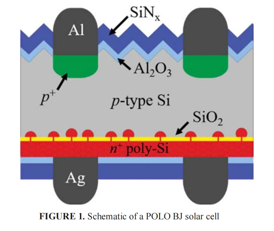
In 2022, Min Byungsul's team at ISFH (the Institute for Solar Energy Research Hamelin, Germany) published a study in AIP Conference Proceedings that took this problem apart. They used POLO passivating contacts — the academic name for what industry calls TOPCon, essentially an ultra-thin oxide plus doped polysilicon poly-Si/SiOx structure — to isolate what's really going on.
The main takeaway isn't complicated: SiNx thickness and firing temperature are a matched pair. Change the thickness and you have to adjust the temperature. Move one without moving the other and either Voc drops or FF collapses.
Technical Parameters
How the experiment was set up
ISFH used p-type CZ wafers, with an n⁺ POLO contact on the cell rear (tunnel oxide plus phosphorus-doped polysilicon).
The two key variables:
Rear SiNx capping thickness — ranging from 40nm to 80nm
Peak firing temperature — adjusted between 790°C and 810°C
They then measured two things: contact resistivity ρc (by TLM) and cell IV parameters.
Earlier we looked at a 2016 JA Solar paper on how the chemical composition (Si/N ratio) of the front-side SiNx anti-reflection film affects silver paste contact. This 2022 ISFH work is about how the physical thickness of the rear-side SiNx capping affects silver paste contact. Put the two together and you cover both dimensions — "chemical composition" and "physical thickness," front film and back film.
All samples fired at 800°C, only rear SiNx thickness varied
| SiNx Thickness | Median ρc (800°C) | Status |
|---|---|---|
| 40nm | ~1 mΩ·cm² | Very low |
| 50nm | ~1.5 mΩ·cm² | Starting to rise |
| 60nm | ~7 mΩ·cm² | Clearly rising |
| 70nm | ~30-40 mΩ·cm² | Transition zone, steep climb |
| 80nm | ~600 mΩ·cm² | Nearly 600x higher than at 40nm |
Firing temperature scan on 55nm and 60nm samples
| Condition | Median ρc |
|---|---|
| 55nm SiNx + 800°C | 3.2 mΩ·cm² |
| 60nm SiNx + 805°C | 2.8 mΩ·cm² |
| 60nm SiNx + 810°C | 2.0 mΩ·cm² |
Technical Advantages
First finding: too thick and the paste can't fire through
All samples fired at a 800°C peak, changing only the rear SiNx capping thickness. The pattern is clear from the table above — the amount of SiNx the paste can burn through during firing is limited. Cross that limit and the paste never reaches the polysilicon below, so contact resistance takes off.
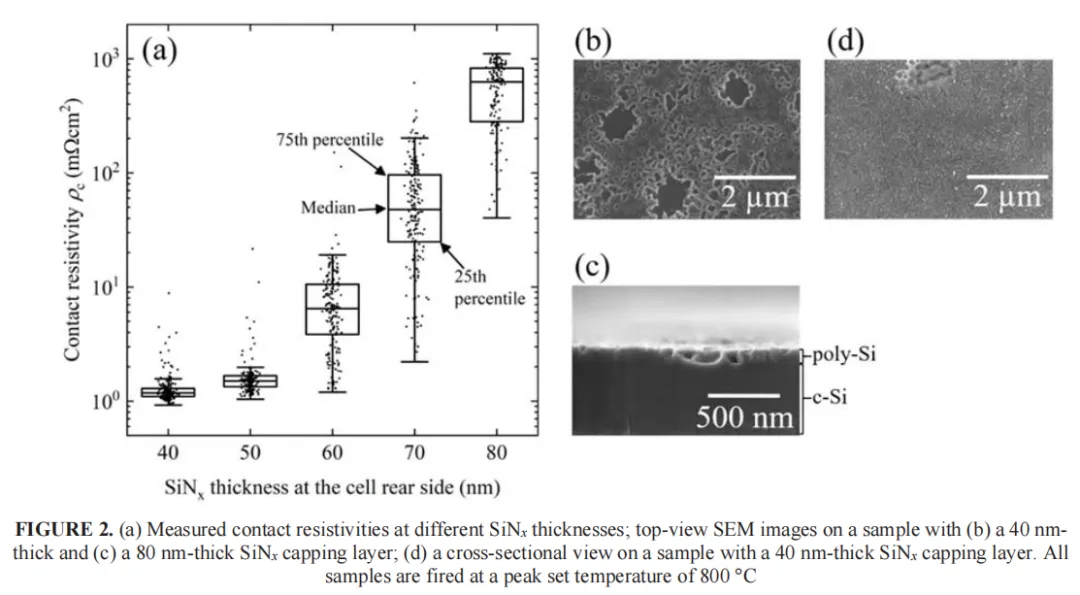
The SEM images give direct evidence:
40nm SiNx: the paste fully burned through both the SiNx and the polysilicon, leaving plenty of micron-scale etch pits on the poly. The polysilicon was locally removed entirely — good contact, but the passivation layer got damaged.
80nm SiNx: only a tiny number of very small etch pits, no regions where the poly was fully removed — passivation held, but contact resistance was nearly 600x higher (about 2.8 orders of magnitude), and FF was basically wrecked.
ISFH's conclusion is blunt: there's an optimal SiNx window — between 50 and 60nm. Too thin, the paste punches through the passivation and Voc craters. Too thick, the paste can't get through and contact resistance flies.
Second finding: thickness and temperature are paired
ISFH didn't stop at "50-60nm is best." They asked a more practical shop-floor question: if the SiNx thickness changes, does the firing temperature need to change too?
They picked 55nm and 60nm groups and ran a temperature scan from 790°C to 810°C.
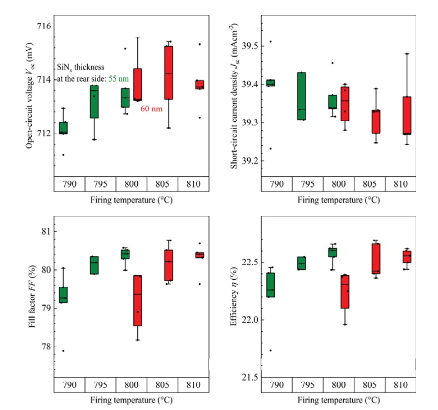
The result is very clean:
55nm SiNx: FF peaks at 800°C, best efficiency there. Go lower and the contact isn't good enough; go higher and passivation starts to suffer.
60nm SiNx: FF peaks at 805-810°C. Because the SiNx is thicker, it needs a higher temperature for the paste to fire through.
In plain line terms: under these test conditions, going from 55nm to 60nm shifts the optimal firing temperature up by about 5-10°C. That slope is only a reference for the same paste system — switch pastes and you need to re-calibrate.
The contact resistivity data back this up too: higher temperature, better contact — as long as you don't cross the line where you start burning through the passivation.
The mechanism: etch pit size is the key
ISFH used SEM to lay out a very clear criterion:
Pits larger than 1μm diameter: poly fully removed, passivation damaged → Voc drops
Pits smaller than 1μm diameter: poly not fully removed, passivation intact → contact resistance falls, Voc unchanged
ISFH put it directly: "a certain number of small-sized etch pits is necessary to form good contact. Etch pits below 1μm in diameter seem to have no effect on passivation quality."
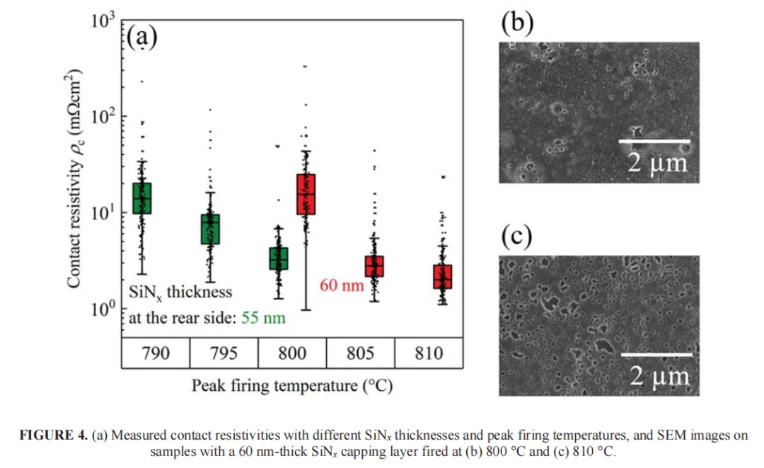
Line criterion: etch pits aren't better fewer, and aren't better more — the target is small size, moderate distribution. If you see lots of >1μm pits under the microscope, the temperature is too high or the SiNx too thin, and the passivation is already taking damage.
Product Application
What can a production line actually use?
1. SiNx thickness isn't better thin, and isn't better thick. Below 40nm, the paste burns through the passivation and Voc craters; above 80nm, the paste can't fire through and contact resistance climbs nearly 600x.
2. Thickness and temperature are paired. Change the SiNx thickness and the firing temperature has to follow. ISFH's data gives a reference — under these conditions, every extra 5nm of SiNx moves the peak temperature up about 5-10°C — but re-calibrate after switching pastes.
3. Etch pits are a "window" indicator. Look at pit size and density by SEM and you can judge whether your current thickness-temperature combination sits inside the window. Lots of >1μm pits → too hot or film too thin; almost no pits → too cold or film too thick, contact may be a problem.
4. Back-film thickness also governs cosmetic yield, and paste selection. The three points above are all about how thickness affects contact resistance and FF through the paste firing through or not. But on the line, rear SiNx thickness controls far more than electrical performance.
In real mass production, rear SiNx is typically controlled in the 70-85nm range — thicker than the 50-60nm "contact optimum" in the ISFH paper. The reason is simple: the paper measured the pure contact optimum for its specific POLO structure and a particular paste, while a production line has to balance passivation, contact and color uniformity all at once, and picks a thicker, more stable range. More importantly, commercial line pastes use a different glass-frit system than ISFH's lab paste, so the SiNx thickness window that can be burned through is different too.
Change the thickness and the refractive index changes, and the interference color of the film shifts with it. Too thin or too thick and the wafers show color variation, off-color and similar cosmetic downgrades that directly cut cosmetic yield. That in turn puts a hard requirement on the paste maker: the paste must match the back-film process window, not force the back film to accommodate one particular paste. Thickness and temperature must pair, and paste and film thickness must pair too — the line is a system, not a single-point tweak.
Three things the paper didn't say
The relation between POLO and TOPCon. The POLO contact ISFH used is essentially ultra-thin oxide plus doped polysilicon (poly-Si/SiOx), basically the same as today's TOPCon rear structure, so the conclusions transfer directly. POLO is the academic name ISFH proposed; TOPCon is the industry-standard term; same structure at heart.
Paste model affects penetration depth. Different pastes have different glass-frit compositions and can burn through different SiNx thicknesses. ISFH's 50-60nm is based on one specific paste — swap pastes and you may need to re-calibrate.
Long-term reliability isn't covered. Will small etch pits grow into big ones over 25 years of outdoor aging? Will the interface degrade further under damp heat? The paper doesn't answer.
Reading it together with JA Solar 2016
| Dimension | JA Solar 2016 | ISFH 2022 |
|---|---|---|
| Application | Front SiNx anti-reflection film (ARC) | Rear SiNx capping layer |
| Focus | Chemical composition of SiNx (Si/N ratio) | Physical thickness of SiNx |
| Core variable | SiH₄/NH₃ gas ratio | SiNx thickness + firing temperature |
| Failure mode | Off Si/N ratio → frit viscosity imbalance → high contact resistance | Wrong thickness → burn through or fail to burn through |
| Fix direction | Tune the gas ratio to the optimal window | Pair thickness and temperature |
| Shared mechanism | Frit-SiNx reaction kinetics decide contact quality | Frit-SiNx penetration depth decides contact quality |
Put the two papers side by side and you get the full picture of front-film and back-film process: chemical composition decides whether you can contact well, physical thickness decides whether you hurt what's underneath while contacting.
Nudge the coating Si/N ratio and Rs spikes, FF collapses, efficiency craters
A reminder for the line: don't only stare at poly when hunting for efficiency loss
With both papers done, back to our own line. When chasing efficiency loss, an engineer's reflex is to first check rear poly thickness, doping level, tunnel oxide thickness — their impact on FF and Voc is well understood and these are standard check items. But the rear SiNx capping layer often gets waved off as a "passivation/cosmetic layer," and few people think of it in terms of contact resistance.
The value of this ISFH paper is exactly that it drags this overlooked variable back onto the table: wrong back-film thickness, paste doesn't fire through or burns through, and FF collapses all the same. Next time you hit a "poly parameters untouched, yet FF mysteriously dropped" situation, don't just circle around the poly — go back and check whether back-film thickness and firing temperature still pair.
Worth noting: ISFH's experiment is based on conventional firing. The LECO technology now widely adopted on lines can optimize contact through a subsequent laser/current step, which to some extent reduces sensitivity to the firing-temperature-thickness pairing — but back-film thickness is still the base window and can't be ignored.
Ooitech's View
We see the same thing on every TOPCon line we commission — the rear SiNx capping gets treated as just a color film, and then FF quietly slips with nobody checking the thickness-temperature pairing. The ISFH data lines up with what pushes people toward LECO, since decoupling contact formation from the firing step buys real margin when your paste's frit chemistry and your back-film window don't perfectly agree. If you want to see how these steps play out on a real module line — coating, firing, stringing and all — the Ooitech YouTube channel at www.youtube.com/ooitech is worth a follow. And keep in mind this is a cell-level study; the module line inherits these cells but the contact fate is already sealed upstream.
References
Min B. et al., AIP Conf. Proc. 2487, 020014 (2022) (DOI: 10.1063/5.0089239)
Chen X.Y. et al., Solar Energy 126 (2016) 105–110 (DOI: 10.1016/j.solener.2016.01.001)