Above 26.3% Efficiency: What's Left on the Rear?
Table of Contents
Quick answer: Above 26.3% cell efficiency, the front of a TOPCon cell is close to optimised and the remaining headroom sits on the rear. That is what drives the shift toward full-area p-type rear contacts and local poly-silicon fingers, which change how the rear collects current and how much area is given to passivation versus contact. The measured structures involve a rear stack with layers around 1 nm, 1.5 nm, 36 nm and 90 nm, a full-area contact and a rear process step near 650 °C, with open-circuit voltages reported at 1.961 V for the devices discussed. Each of those dimensions trades contact resistance against recombination, and the optimum moves as the front improves. On a line, this means the rear recipe becomes a live variable rather than a fixed part of the process.
PV Module Manufacturing · by Jerry, Ooitech
Above 26.3% Efficiency, What Is Left to Optimize on the Rear?
“Lao Zhang, the 26.66% cell used a full p-type TOPCon rear structure. In the 26.34% paper, the front was changed to localized n-TOPCon fingers, while the rear became a full-area p-TOPCon contact. Is the double-layer SiOx/poly-Si stack still the same?”
That was the follow-up question from our process team after we finished discussing the 26.66% cell yesterday.
The basic rear double-layer architecture is almost copied from the 26.66% design, but the p-TOPCon side introduces three adjustment knobs that the 26.66% cell did not touch. The front-side strategy is also completely different. It moves away from the 430 Ω/□ high-resistance boron emitter and toward localized n-TOPCon fingers. These are two very different approaches to reducing recombination.
The 26.34% paper by Gao K. et al. can be viewed as the back-junction sister study of the 26.66% work. Reading the two together gives a clearer picture of what may be required to approach 27% efficiency.
Gao, K. et al. “Bifacial tunnel oxide passivating contacts for silicon and perovskite/silicon tandem solar cells with improved efficiency.” Nature Energy (2026). DOI: 10.1038/s41560-026-02007-8
Three Numbers Behind the 26.34% Cell
Single-junction efficiency: 26.34% on 335.5 cm², with a Voc of 743.2 mV, FF of 85.0% and Jsc of 41.69 mA/cm².
Tandem efficiency: 32.73%, using a 1.68 eV perovskite top cell. The tandem Voc reached 1.961 V, while 80% of the initial performance remained after 2,000 hours of MPP tracking.
Structural definition: front localized n-TOPCon fingers in a back-junction layout, combined with a full-area double-layer p-TOPCon rear contact. This is essentially a mirror inversion of conventional TOPCon, which normally uses a front boron emitter and a rear n-TOPCon contact.
Rear Double-Layer Contact: The Same Skeleton, but Three Different Process Knobs
The 26.66% rear contact uses SiOx / lightly doped n+ poly-Si / SiOx / heavily doped n+ poly-Si, with phosphorus as the dopant.
The 26.34% rear contact uses SiOx / p+ poly-Si at 36 nm / SiOx / p+ poly-Si at 90 nm, with boron doping.
Both structures follow the same basic sequence: bottom SiOx, inner poly-Si, intermediate SiOx and outer poly-Si. The p-TOPCon version, however, must deal with a long-standing problem.
p-TOPCon has always faced a passivation-versus-contact trade-off. Boron can generate more defects at the Si/SiO₂ interface than phosphorus, while the metallization of p+ poly-Si is more difficult because of hole transport limitations and the weaker interaction between conventional silver paste and p+ poly-Si.
| Comparison item | 26.66% rear contact: full-area n-TOPCon | 26.34% rear contact: full-area p-TOPCon |
|---|---|---|
| Dopant polarity | Phosphorus, n+ | Boron, p+ |
| Inner / outer poly-Si thickness | Approximately 40 / 60 nm | 36 / 90 nm; the thicker outer layer provides more margin for boron diffusion and metallization |
| Intermediate SiOx | Approximately 1.5 nm, thermally oxidized at 620°C | Approximately 1 nm, formed by in-situ thermal oxidation at 650°C; thinner because hole tunnelling is already more difficult on the p+ side |
| Annealing | Estimated 880–920°C range in the previous analysis | Pre-annealing at 1050°C for more than 30 seconds, achieving 98% crystallinity and pushing implied Voc to 747 mV |
| Silver paste | Conventional paste, paired with an outer amorphous layer to limit Ag penetration | Alkali-metal-oxide-modified paste with 4 wt% Na₂O/K₂O and rough silver powder, reducing contact resistivity to 0.55 mΩ·cm² |
| Rear morphology | Conventional rear polishing | Planarized rear polishing because p-TOPCon is more sensitive to surface texture and requires lower J₀ |
| Main target | Block Ag penetration while maintaining passivation | Block Ag penetration, suppress boron-related interface defects and improve p+ poly-Si metallization |
The reported process data include in-situ rear oxidation at 650°C, an approximately 1 nm intermediate SiOx layer, boron doping of 1 × 10²⁰ cm⁻³, 98% crystallinity after 1050°C pre-annealing, an implied Voc of 747 mV, and a contact resistivity of 0.55 mΩ·cm² using an alkali-metal-modified paste with rough silver powder.
One detail is easy to miss. The outer p+ poly-Si layer is 90 nm thick, 50% thicker than the roughly 60 nm outer layer used on the n-TOPCon side.
This is not an arbitrary increase. Boron has a lower solid solubility in poly-Si than phosphorus, so the heavily doped section needs more thickness to reduce contact resistivity. At the same time, the 1050°C pre-annealing step drives boron inward. A thicker outer layer helps prevent boron from penetrating and damaging the bottom SiOx layer.
That is the opposite of the n-TOPCon strategy, where the outer layer can remain thinner and more amorphous.
Front Side: The 430 Ω/□ Strategy Is Replaced by Localization
The question left by the previous study was whether the 430 Ω/□ high-resistance boron-emitter strategy would still apply to a fingered n-TOPCon front contact.
The answer from the 26.34% cell is clear: it does not. The design moves onto a different track.
The 26.66% cell uses a conventional boron-diffused front emitter with a sheet resistance of 430 Ω/□. Fine metal fingers of around 10 μm compensate for the weaker lateral conductivity.
The 26.34% cell removes the conventional front boron emitter and replaces it with patterned n-TOPCon fingers approximately 210 μm wide, leaving poly-Si only beneath the metal-contact regions.
The recombination-reduction mechanism therefore changes from diluting the dopant concentration through a high sheet resistance to reducing the area covered by poly-Si.
The texture is modified first. Ozone and HF are used to round the pyramid tips. This reduces poor passivation and silver-paste corrosion around sharp texture peaks.
A gradient thermal field, or GTF, is introduced into LPCVD. The Raman full width at half maximum reaches 8.4 cm⁻¹. A lower value indicates better crystallinity. The gradient thermal field improves both lateral and vertical temperature uniformity and raises the crystallinity of the n+ poly-Si.
Phosphorus doping reaches 3.3 × 10²⁰ cm⁻³. This is about one order of magnitude higher than the phosphorus concentration used in the 26.66% rear contact. The front n+ fingers are designed for conductivity rather than full-area passivation. Most of the passivation work is carried by the full-area rear p-TOPCon contact.
The finger width is approximately 210 μm. Poly-Si remains under the metal, while the non-contact textured area is left uncovered. This substantially reduces front-side parasitic absorption compared with a full-area poly-Si contact.
The 430 Ω/□ approach belongs to the boron-emitter era. In a fingered n-TOPCon structure, recombination is controlled through localized poly-Si coverage, rounded surface texture and improved crystallinity from GTF-LPCVD, rather than simply increasing sheet resistance.
This helps explain how the 26.34% cell reaches a Voc of 743.2 mV, close to the 744.6 mV reported for the 26.66% cell, while also achieving a higher Jsc. The localized front contact cuts parasitic absorption that would remain in a full-area front poly-Si structure.
Side-by-Side Comparison of the Two 26% Sister Designs
Rear Double-Layer SiOx/poly-Si Contacts
| Layer or process | 26.66% n-TOPCon rear | 26.34% p-TOPCon rear | Main reason for the difference |
|---|---|---|---|
| Bottom SiOx | Approximately 1.3–1.6 nm, formed in O₂ at 620°C | Approximately 1.8 nm, formed in situ at 650°C | The p-type side needs a stronger barrier against boron penetration, even though hole tunnelling is more difficult |
| Inner poly-Si | Approximately 40 nm, lightly phosphorus-doped and highly crystalline | 36 nm, lightly boron-doped | Boron has lower solid solubility; a thinner inner layer can still support passivation |
| Intermediate SiOx | Approximately 1.5 nm, formed in O₂ at 620°C | Approximately 1 nm, formed in situ | Tunnelling is more demanding on the p-type side, so the intermediate layer cannot be too thick |
| Outer poly-Si | Approximately 60 nm, heavily phosphorus-doped and mainly amorphous | 90 nm, heavily boron-doped | p+ poly-Si metallization is more difficult, requiring a thicker layer and modified paste |
| Annealing | Approximately 880–920°C | 1050°C pre-annealing, reaching 98% crystallinity | Boron requires a higher activation temperature, while the process must also control boron-related interface defects |
| Silver paste | Conventional paste paired with an amorphous outer layer | 4 wt% alkali-metal oxide plus rough silver powder | Metallization of p+ poly-Si remains one of the main process bottlenecks |
Front-Side Comparison
| Item | 26.66% front side | 26.34% front side |
|---|---|---|
| Structure | Full-area boron-diffused emitter | Localized n-TOPCon fingers approximately 210 μm wide |
| Recombination-control strategy | High sheet resistance of 430 Ω/□ to dilute doping | Reduced poly-Si coverage combined with rounded texture |
| Surface texture | Conventional inverted-pyramid texture | Ozone- and HF-treated rounded pyramids |
| Poly-Si deposition | Not applicable | GTF-LPCVD with Raman FWHM of 8.4 cm⁻¹ |
| Dopant | Boron | Phosphorus at 3.3 × 10²⁰ cm⁻³ |
What the Two Papers Say About Rear-Contact Development Above 26%
The combined message is fairly direct.
At the 25% level, the focus was the pinhole behavior of the oxide layer. At the 26% level, development moved toward double-layer SiOx/poly-Si structures and metallization engineering. Above 26.3%, the routes begin to split: n-TOPCon rear contacts pursue bifacial electrical synergy, while p-TOPCon rear contacts move toward a back-junction layout with localized front fingers. The latter is already close to a partial BC-TOPCon architecture.
The intermediate SiOx layer used to block silver penetration is a shared feature of both double-layer rear-contact designs. The p-TOPCon side, however, must solve three additional problems:
A 1050°C pre-annealing step is needed to activate boron, increase crystallinity and suppress boron-related interface problems.
Alkali-metal-oxide-modified silver paste is needed to address the difficult metallization of p+ poly-Si.
Rear-side polishing and planarization become more critical because p-TOPCon is more sensitive to surface texture and its effect on J₀.
These issues were not central to the 26.66% n-TOPCon design. Put simply, the double-layer p-TOPCon contact is more difficult to manufacture than its n-TOPCon counterpart, but it may offer higher Voc potential once the process is controlled.
The double-layer rear p-TOPCon contact in the 26.34% cell reached an implied Voc of 747 mV, slightly higher than the estimated overall implied Voc level discussed for the 26.66% design.
Production-Line Parameters That Can Be Applied Directly
Improve rear polishing and planarization. A p-TOPCon production line should not treat rear polishing as a process that only needs to be “good enough.” Planarization has a stronger influence on the J₀ of the double-layer p-TOPCon contact than it does on n-TOPCon.
Form the intermediate SiOx layer in situ at approximately 1 nm. Copying the 1.5 nm thermal oxide used in the 26.66% n-TOPCon structure may reduce tunnelling and hurt FF on the p-type side.
Introduce a 1050°C pre-annealing step. Without this treatment, boron activation and 98% crystallinity are difficult to achieve, making an implied Voc of 747 mV unlikely.
Use an alkali-metal-oxide-modified silver paste. The reported formulation uses 4 wt% Na₂O/K₂O and rough silver powder. A contact resistivity of 0.55 mΩ·cm² is a hard target for the p-TOPCon side. Conventional paste can cause series resistance to rise sharply at the p+ contact.
Control the front finger width at approximately 210 μm. Laser patterning accuracy must keep pace with the narrower contact geometry. Reducing the finger width further could cut parasitic absorption again, but laser damage to the double-layer stack would need to be reassessed.
The Next Question for BC-TOPCon
The 26.34% structure, with front n-TOPCon fingers and a full-area double-layer p-TOPCon rear contact, is effectively a partial version of BC-TOPCon.
The next logical step would be to localize the rear p-TOPCon contact as well, arranging rear p-type fingers and n-type fingers in an interdigitated pattern. That would create a true BC-TOPCon structure.
This raises a new question. Should the intermediate SiOx layer in the localized rear p-TOPCon contact remain pure SiO₂, or should it be replaced by nitrogen-doped SiOx following an OGO-type route to strengthen field passivation? Another option would be an AlOx/SiOx stack, using the field effect of aluminum oxide together with the double-layer SiOx/poly-Si contact.
The 26.34% study did not explore this issue because its rear p-TOPCon contact remained full-area and did not depend on localized field-effect passivation. Once the rear p-type contact becomes fingered, however, the combination of AlOx field-effect passivation and a double-layer SiOx/poly-Si structure may become a serious next-step option.
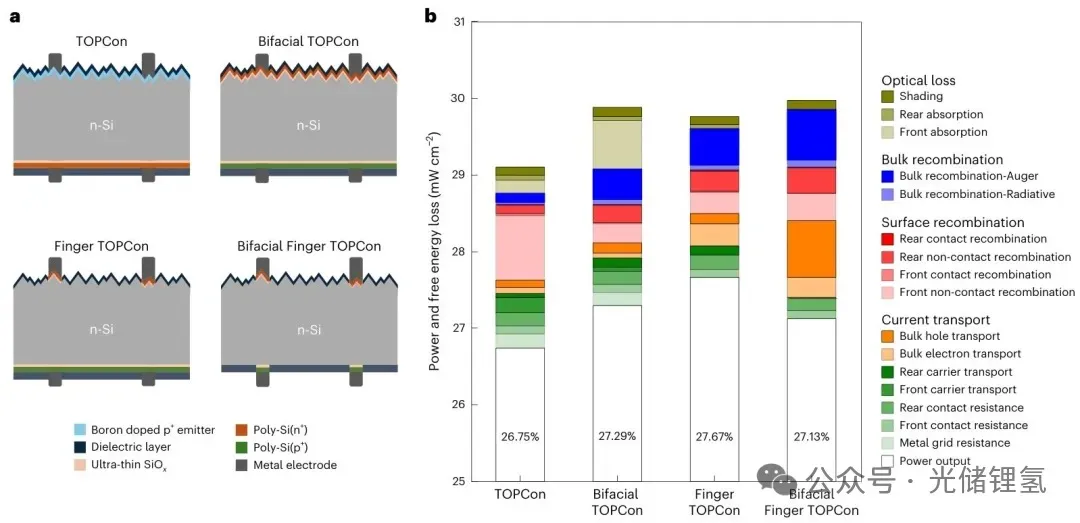
There is also a tandem-related process question. The bottom cell used in the 32.73% tandem has a textured front surface. Simulations in Figure 1 indicate that a double-sided finger-TOPCon configuration may have higher tandem potential than a full-area double-sided TOPCon structure.
But how should photoluminescence uniformity be controlled across a textured front surface with localized n-TOPCon fingers? Excessive laser energy can locally burn or flatten the pyramid tips. That may consume part of the process window created by the rounded-pyramid treatment.
Across the three studies—from the 25.4% Das Solar cell to the 26.66% and 26.34% cells—the rear-contact logic has moved through three generations: oxide pinhole control, double-layer protection against silver penetration, and finally double-layer p-TOPCon combined with alkali-metal-modified metallization.
Ooitech's View
The process window is the real bottleneck here. Once p-TOPCon moves from a full-area rear contact toward localized BC fingers, contact resistivity, laser damage, boron activation and field-effect passivation will have to be optimized as one coupled system. A thinner intermediate SiOx layer may protect FF, but it also leaves less margin against silver penetration and boron-driven interface damage. The next useful result will be one that demonstrates this complete integration window on production-size wafers, not only a peak efficiency value.
Further reading and background data
Public reference material on this topic, published by the organisations that maintain the industry's technology roadmap and market data: