High-Sheet-Resistance Emitters
Table of Contents
Quick answer: High-sheet-resistance emitters are widely assumed to raise cell efficiency, because a lighter doping level reduces recombination in the emitter and lets more short-wavelength light through to be converted. The assumption is only partly right. Raising emitter sheet resistance does reduce recombination, but it also raises the contact resistance between the emitter and the screen-printed silver fingers, and it narrows the process window for firing. Past a certain point the two effects cancel and further gains require better contact formation rather than lighter doping. This is why high-sheet-resistance emitters have moved into production alongside advances in paste formulation and firing profiles rather than on their own. On a TOPCon line the emitter interacts with the rear passivating contact, so the optimum is set by both sides at once.
PV Module Manufacturing · by Jerry, Ooitech
Product Introduction
Everyone in the PV world takes it as a given: pushing up emitter sheet resistance (Rsheet) buys you higher Voc, but you pay for it with a collapsing fill factor. So the first question is simple. Did high sheet resistance actually break the FF this time?
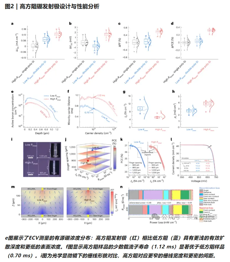
Look at the box plots in figures a through d. The data is a bit counter-intuitive.
High-Rsheet single poly-Si versus low-Rsheet single poly-Si: Jsc barely moves, ΔJsc is close to 0. Voc ticks up a little. And FF, instead of dropping, actually creeps up.
High-Rsheet double poly-Si is the full package. Against the low-Rsheet single poly-Si baseline, Jsc gains about 0.12 mA/cm², Voc gains about 2 mV, and FF is dragged up by roughly 0.4%.
The takeaway: the high-sheet-resistance emitter did not bring the transport penalty everyone feared. Through structural optimization, it lifted the whole set of electrical parameters instead.
Technical Parameters
From "dead layer" to fine grid: the precision surgery
Figures e and f reveal the physics behind it.
First, kill the dead layer and double the lifetime. The ECV (electrochemical capacitance-voltage) profile in figure e shows that the surface boron concentration of the high-Rsheet emitter (red curve) sits well below the low-Rsheet one (blue curve). That means the surface "dead layer", the lattice-damaged region caused by heavy doping, gets thinner.
This shows up in the effective minority carrier lifetime in figure f. The low-Rsheet sample only reaches 0.70 ms at an injection level of 10^15 cm^-3, while the high-Rsheet sample jumps straight to 1.12 ms. Longer minority carrier lifetime pulls the recombination current density J0 down (see figure g), which gives the Voc gain a solid foundation.
| Parameter | Low-Rsheet emitter | High-Rsheet emitter |
|---|---|---|
| Minority carrier lifetime (at 10^15 cm^-3) | 0.70 ms | 1.12 ms |
| Grid line pitch | 1120 μm | 825 μm |
| Grid line width | 20 μm | 10 μm |
| J0 (double poly-Si) | higher | ~5 fA/cm² |
| Contact resistivity ρc (double poly-Si) | — | ~2-3 mΩ·cm² |
High sheet resistance alone is not enough, you still have to fix lateral transport. Compare the micrographs in figure i. The low-R emitter has a grid pitch of 1120 μm and a line width of 20 μm. The high-R emitter tightens the pitch to 825 μm and shrinks the line width to 10 μm. That is the essence of the grid redesign: since emitter resistance went up, make the grid denser and finer to add more conductive paths, while the thinner fingers cut shading area. This fine design not only cancels the loss from high sheet resistance, it also improves optical capture.
Technical Advantages
The deep trade-off between electrical parameters
Figures g and h cover the two parameters a line engineer cares about most.
Recombination current density (J0): the high-Rsheet double poly-Si (red dots) has the lowest J0, roughly 5 fA/cm², well below the other groups. This says the double poly-Si structure effectively blocks metal impurity diffusion and protects the interface passivation.
Contact resistivity (ρc): a high-sheet-resistance emitter normally drives contact resistance up. But in figure h the high-Rsheet double poly-Si (red dots) still holds ρc at a low level, about 2-3 mΩ·cm². Through optimized metallization (LECO or nano-second Joule heating, for example), a high-sheet-resistance emitter can still form a good ohmic contact, and there is no "high resistance meets high resistance" FF disaster.
Product Application
Three hard numbers for the production line
Pulling together the simulation and measured data in figures j to l, here are a few landing points for the PE (process engineers) and PD (product developers).
A new anchor for sheet resistance: the traditional 100-200 Ω/□ may not be the optimum. The data suggests pushing to around 430 Ω/□ (red curve in figure e) gives the best lifetime and Voc payoff. But it needs excellent tube furnace uniformity, otherwise the edge effect blows up.
The grid design trade-off: shrinking line width from 20 μm to 10 μm puts huge demands on screen-printing alignment accuracy and silver paste rheology. The simulation surface in figure k shows an optimal matching zone between grid pitch and emitter sheet resistance, and blindly narrowing the fingers sends series resistance soaring.
The "invisible armor" of double poly: the current density-voltage (JV) curve in figure l shows the high-Rsheet double poly-Si curve is the fullest, with no obvious kink. That proves the double-layer structure works at suppressing parasitic leakage, so high Voc actually converts into high PCE.
Contact and Discussion
A brick thrown to peers
We chase high sheet resistance on the front surface (for Voc) and fine grids (to hold FF), and double poly on the rear surface (to suppress Ag penetration and lift bifaciality). Once you stack this "both-sides-to-the-extreme" combination, the process window gets squeezed very tight.
High-resistance boron diffusion on the front puts extreme demands on PSG cleaning and boron source deposition uniformity. The rear double poly needs equally high precision in CVD deposition and laser grooving.
Here is the real question. As cell efficiency creeps toward the 26.7% theoretical limit, should we spend more energy on micro-uniformity control of the equipment (the tube furnace thermal field for boron diffusion, the flatness of the CVD loading stage) rather than endlessly piling on new process steps? For those of you grinding it out on the line, what do you think is the biggest bottleneck holding back volume production of high-Rsheet emitters plus double poly, the equipment capability or the process-integration mindset?
Ooitech's View
Honestly, the story here is less about a new process step and more about how tight the window gets when you push both surfaces at once. A 10 μm finger over a 430 Ω/□ emitter lives or dies on print alignment and furnace uniformity, so the fight really moves from "what recipe" to "how repeatable is my hardware." On a module line the same logic bites at stringing and interconnection, where fine, fragile fingers punish sloppy handling. Worth a subscribe to the Ooitech YouTube channel (www.youtube.com/ooitech) if you want to see how this uniformity obsession plays out on the floor.