BC Solar Cells Explained: Structure, Differences
Table of Contents
Quick answer: A BC solar cell, short for back-contact, is a high-efficiency crystalline silicon cell with both the positive and negative contacts on its rear face. Moving the contacts off the front removes the busbar shading that a conventional cell accepts, so more of the cell area is available for light, and it also removes the need for a front solder ribbon. The cost is a denser rear pattern: because both polarities are interdigitated on the back, the rear metallisation and the isolation between the two contact sets have to be defined much more precisely than on a TOPCon or PERC cell. That rear complexity is what makes BC cells more expensive to produce and more demanding to string, and it is why the architecture has stayed in high-efficiency product tiers rather than moving to the volume market where TOPCon sits.
PV Module Manufacturing · by Jerry, Ooitech
Product Introduction
BC solar cell, short for Back Contact solar cell, is a high-efficiency crystalline silicon cell technology where the emitter, back surface field and metal electrodes are all placed on the rear side of the cell. Its basic form is usually known as IBC, or Interdigitated Back Contact cell.
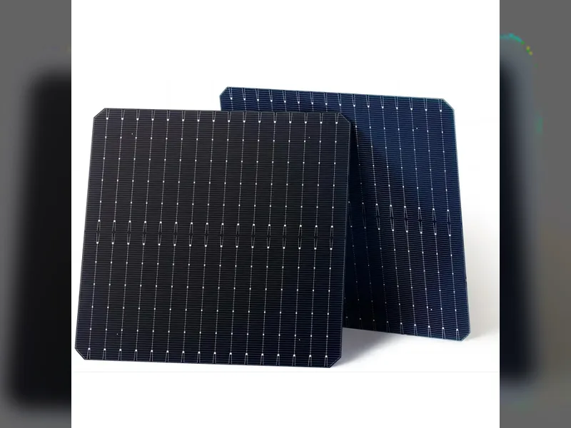
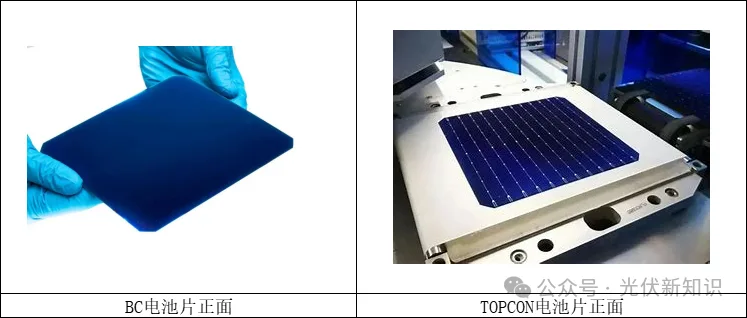
Compared with conventional crystalline silicon cells, the most visible feature of BC cells is that there are no metal grid lines on the front surface. Since the front side is free from busbar and finger shading, more sunlight can enter the cell surface, optical loss is reduced, and the effective power generation area is increased. This is why BC cells are often used for high-efficiency and high-aesthetic solar modules.
What Makes BC Cells Different
The key difference between BC cells and PERC, TOPCon or HJT cells is not simply the wafer type or a single passivation layer. The core idea of BC technology is structural: the PN junction and metal electrodes are moved to the rear side of the cell.
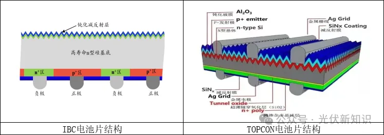
For example, TOPCon is often discussed in relation to N-type silicon substrates, front-side passivation, and rear-side tunnel oxide passivated contact structures. PERC is usually based on rear passivation improvement. HJT uses amorphous silicon passivation and heterojunction contact. BC, however, focuses on removing front-side electrode shading by moving the current collection structure to the back.
Because of this, BC can also be combined with other cell technologies. Pure BC technology is generally represented by IBC. TOPCon plus BC can form TBC technology; HJT plus BC can form HBC technology. HPBC is commonly known as a P-type IBC-related route, while ABC refers to All Back Contact technology, often discussed together with silver-reduction or silver-free design concepts.
Technical Parameters
Typical BC Cell Structure
Taking IBC as an example, the most important structural change is that both the PN junction and the metal electrodes are located on the rear side of the cell. The front surface is mainly used for light absorption and passivation, while the rear surface completes carrier separation and current collection through interdigitated positive and negative regions.
| Item | Description |
|---|---|
| Cell type | Back Contact solar cell |
| Basic technology route | IBC, Interdigitated Back Contact |
| Front side feature | No front-side metal grid line shading |
| Rear side feature | Positive and negative electrodes arranged on the back side |
| Core structural design | PN junction and metal electrodes moved to the rear side |
| Main benefit | Reduced optical shading loss and improved effective light absorption area |
| Compatible routes | IBC, TBC, HBC, HPBC, ABC and other BC-based structures |
| Module process impact | Requires different string soldering logic compared with PERC, TOPCon and HJT cells |
IBC Cell Manufacturing Process
A typical IBC cell process can be summarized as follows:
Chemical polishing and damage removal
BBr3 tube diffusion
Dry oxygen mask growth
Screen printing for local BSF opening
POCl3 tube diffusion
Texturing
Double-side passivation
Screen printing for local contact opening
Screen printing metallization
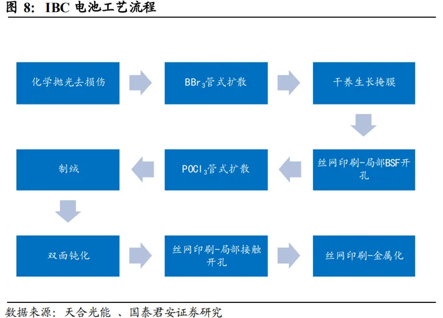
The core challenge of BC technology is how to prepare high-quality p-type and n-type regions on the back of the cell in an interdigitated pattern. In a typical process, a boron-containing interdigitated diffusion mask can be printed on the rear side. After diffusion, boron enters the N-type substrate and forms the p+ region. The area without the printed mask can then form the n+ region through phosphorus diffusion.
On the front side, pyramid texturing is used to enhance light trapping, while a front surface field, often called FSF, is formed to improve electrical performance. This combination of optical management and rear-side carrier collection is one reason why BC technology is attractive for premium modules.
Technical Advantages
No Front-Side Grid Shading
The most direct advantage of BC cells is that the front surface has no metal grid line. This reduces shading loss and increases light utilization. For module appearance, the all-black or near-uniform front surface can also deliver a cleaner visual effect, which is especially attractive in distributed commercial, industrial and building-related PV applications.
Higher Efficiency Potential
Because the front surface can receive more incident light, BC cells have a strong theoretical and practical efficiency advantage. When combined with advanced passivation technologies such as TOPCon or HJT, BC structures can further improve conversion efficiency.
Flexible Technology Integration
BC is not limited to one single cell route. It can work as a platform structure and combine with other high-efficiency technologies. This is why the industry discusses routes such as TBC, HBC, HPBC and ABC. The common direction is the same: reduce optical loss, improve carrier collection, and raise module power output.
Special Rear-Side Grid Design
Since both positive and negative electrodes are located on the back side, the grid layout of BC cells is quite different from conventional cells. The following example uses red lines for positive busbars and blue lines for negative busbars, taking an 18BB rear-side layout as an example.
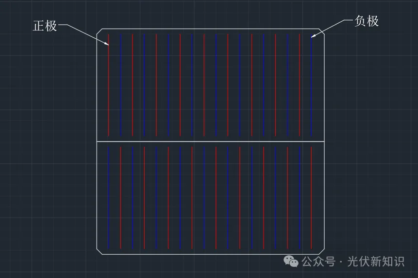
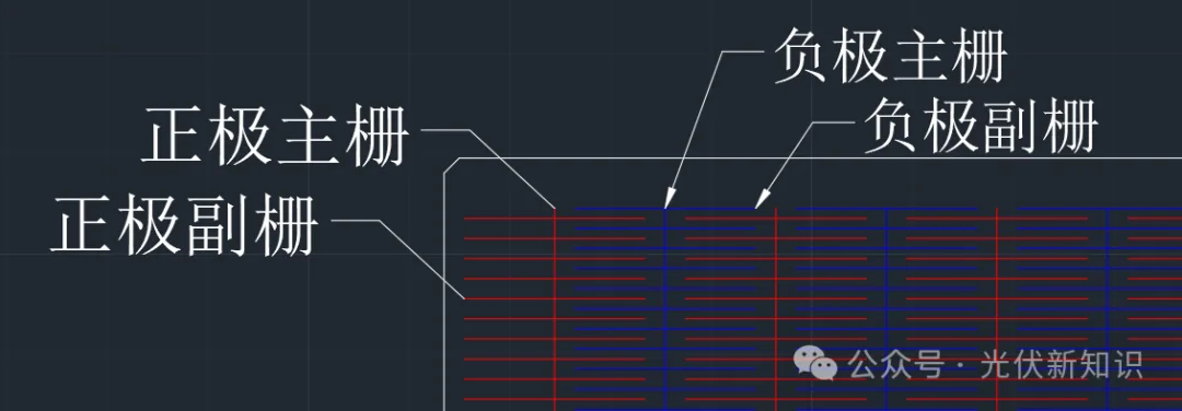
When the fine fingers are also shown, the positive and negative fingers are arranged in an interdigitated pattern. The PN junction regions are also distributed in a similar interdigitated way. The main busbars collect current by crossing and connecting with the corresponding finger structure.
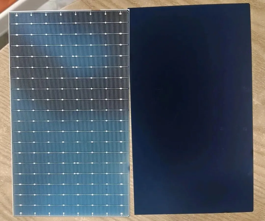
From the real BC cell image, we can see not only the rear-side grid lines, but also PAD points on both sides of the half-cell. These PAD points are important for electrical connection and soldering design, especially in high-density interconnection structures.
Product Application
BC Cell String Soldering Principle
BC cell soldering is different from conventional PERC or TOPCon cell soldering. For common double-side-grid cells, the ribbon usually connects from the rear side of one cell to the front side of the next cell. In BC cells, both positive and negative electrodes are on the rear side, so the soldering ribbon must follow a different connection path.
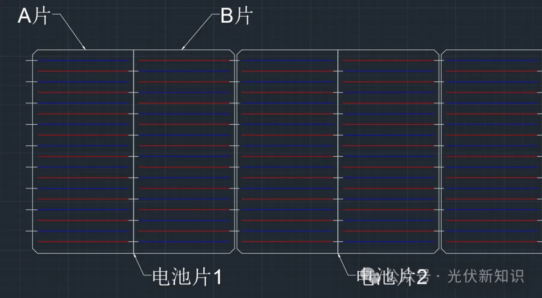
As shown in the diagram, BC string soldering realizes cell series connection by using soldering ribbons in a cyclic and staggered pattern between two adjacent cells. This is different from the welding method used for TOPCon cells, where the ribbon travels from the back of one cell to the front of the next cell.
A full cell can be divided into two half-cells, A and B. The electrodes of the A half-cell and B half-cell are arranged opposite to each other. During BC cell string soldering, the ribbon from the starting cell is pulled to the negative electrode of the A half-cell and then cut. The following connection logic is then repeated:
From the positive electrode of A half-cell on cell 1 to the negative electrode of B half-cell on the same cell
From the positive electrode of B half-cell on cell 1 to the negative electrode of A half-cell on cell 2
Repeat the above cycle to complete the cell string connection
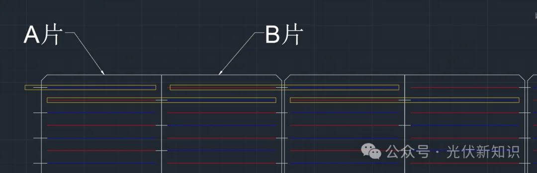
In the highlighted area, the ribbon is actually one continuous ribbon. Different colors are used only to make the positive and negative electrode relationship easier to understand. The diagram clearly shows the cyclic staggered welding pattern on the BC cell.
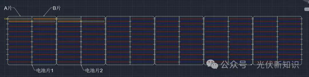
The completed cell string shows how the welding ribbons are arranged across multiple BC cells. This type of stringing requires accurate ribbon placement, stable tension control, precise positioning, and a good understanding of the rear-side electrode pattern.
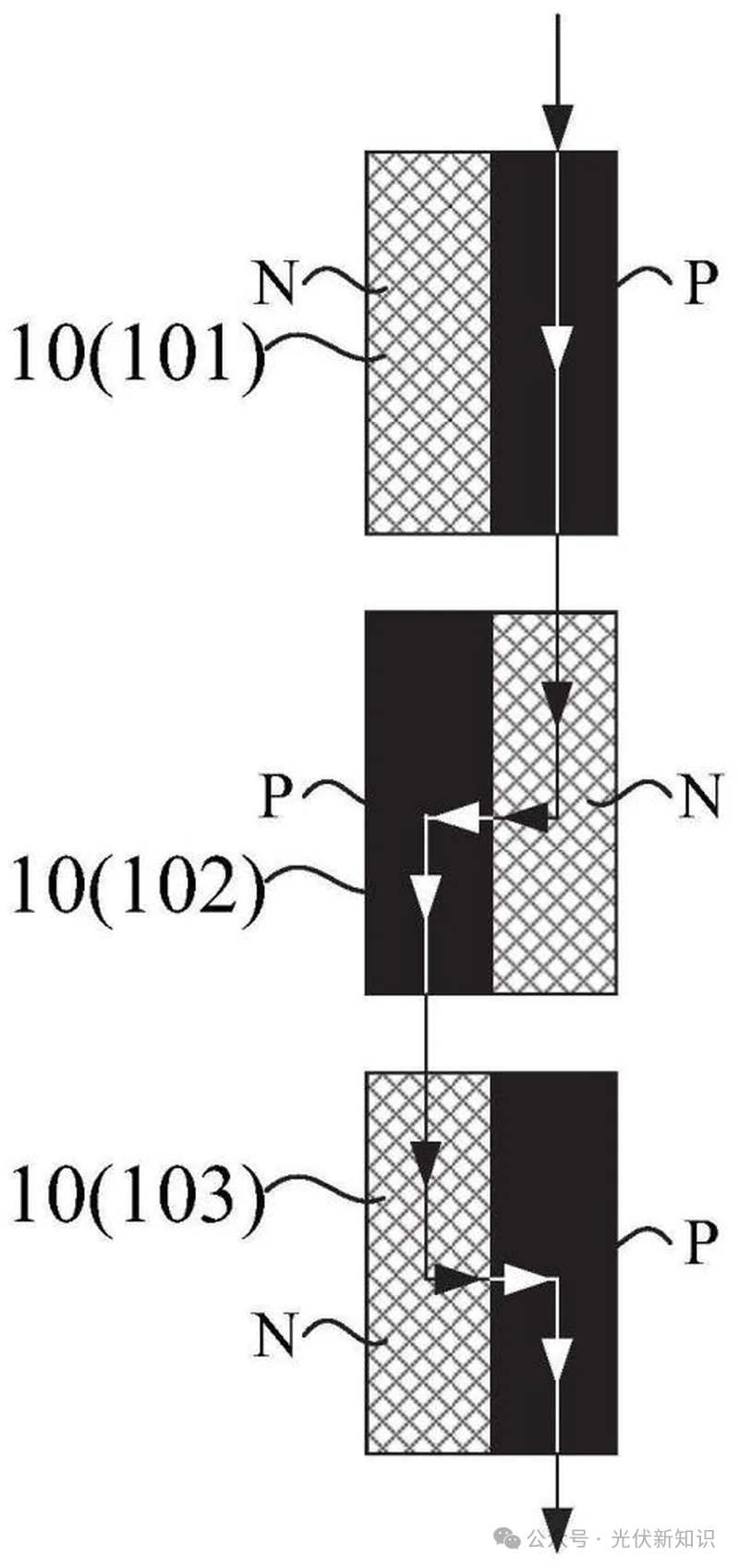
The current flow diagram further explains the series connection principle. Since the current path is formed on the rear side through staggered ribbon routing, BC stringing equipment and process control are more demanding than standard ribbon soldering for traditional cells.
Contact and Purchase
Practical Notes for BC Module Manufacturing
For manufacturers planning to produce BC modules, the cell stringing section is one of the most important process points. The rear-side electrode design means that conventional stringing logic cannot simply be copied. Equipment must support accurate back-contact alignment, controlled ribbon feeding, stable soldering temperature, and reliable inspection after welding.
In production, engineers should pay close attention to ribbon offset, solder joint quality, cell cracking risk, PAD point matching and current path consistency. Any small deviation in rear-side soldering may cause resistance increase, power loss, or reliability issues after lamination and long-term outdoor operation.
Ooitech's View
As an equipment supplier, we see it this way: BC technology is not only a cell-efficiency upgrade, but also a module manufacturing challenge, especially in string soldering accuracy and rear-side interconnection control. For a solar panel production line, the key is to match the stringer design with the real BC cell electrode pattern rather than treating it like a modified TOPCon or PERC process. In our view, factories evaluating BC modules should verify soldering stability, ribbon routing and EL performance at pilot scale before moving to mass production.